
With my first Minimalist Europe Card Bus CPU Card finally completed, to my satisfaction. Next up, is my Motorola based I/O Card, which will finally enable a complete modular 6809 based system.
In fact, my initial design has been completed, which also contributed a couple of recent posts / videos as I finalised the ACIA Baud Rate Generator, and the Interrupt Driver components of the design.
The Motorola based I/O Card includes the following Motorola peripherals:
- A MC6850 Asynchronous Communications Interface Adapter (ACIA)
- A MC6821 Peripheral Interface Adapter (PIA)
- A MC6840 Programable Timer Module (PTM)
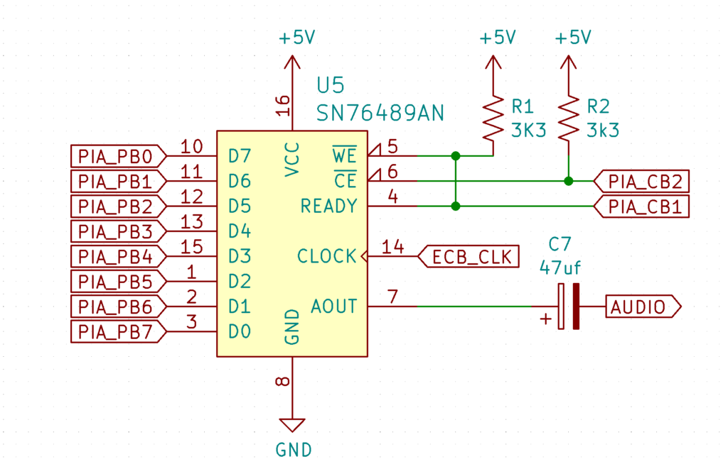
In addition, I’ve added an optional Sound Interface, via a SN76489 Digital Complex Sound Generator, interfaced via one of the PIA ports.
The schematic and PCB layout for the initial prototype have both been completed, and the first prototype PCB’s have just arrived.
Join me, as I walk through the Schematic and PCB layout and then assemble and test my first card.
So, before we get too far ahead of ourselves, let’s start-off by taking a look at the schematic.
Firstly, I (once again) based the design on the MECB KiCAD Template, which I’d initially designed to make the design of subsequent boards easier and consistent.
So, as with my other boards, I started off with the MECB connector and Address Decode PLD already defined in the schematic, and laid-out on the PCB. As always, this is very helpful!
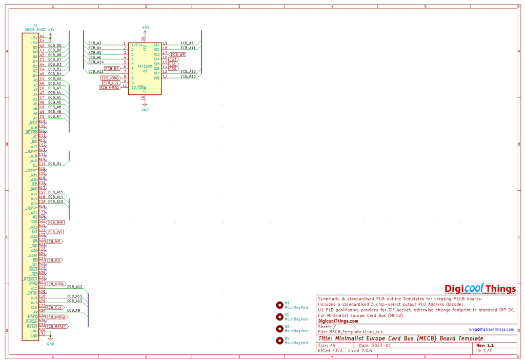
Here’s the completed Motorola I/O Card v1.1 schematic.

Adding the Motorola peripheral chips to the initial KiCAD template was straightforward, with each connecting up to a PLD chip select output.

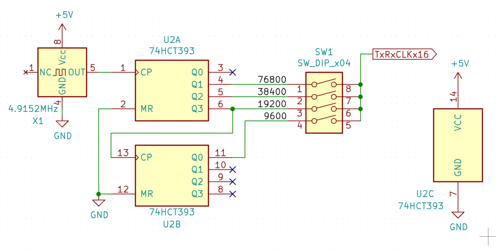
Next was the Baud Rate Generator for the MC6850 ACIA, which I covered in detail in an earlier video.
Then, also covered in an earlier video, is the optional Programmable Timer Module Non-Maskable Interrupt driver.

This allows a Monitor program, that implements it (such as ASSIST09), to support single-stepping of your code and the setting of breakpoints, to allow for easy on-board code debugging.
Finally, I’ve used Port B of the PIA to optionally interface to a SN76489 Sound Generator. It’s optional, as I’ve also brought-out all of the PIA Port pins to a connector.
So, if the Sound is not desired, you can simply not insert a Sound Generator chip, so both PIA ports are available for external use.
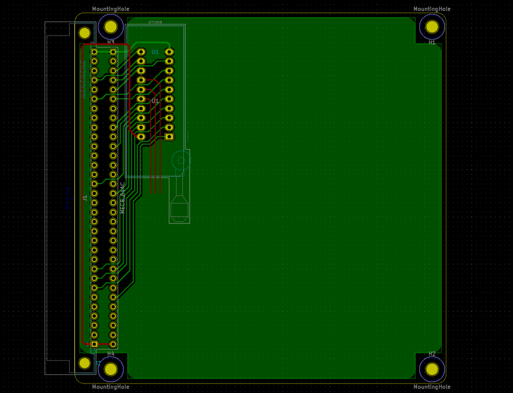
So, let’s now take a look at the PCB layout.
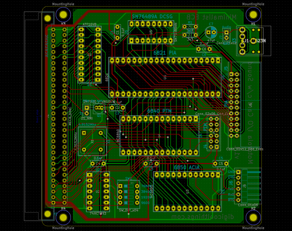
Everything fits quite tidily on the (just under) 100mm square standard MECB card size.
Including connectors for all the I/O connections.
This includes, on the board edge, first a 24 pin right-angle male IDC connector bringing out all 20 I/O pins of the PIA. We also have a 6 pin FTDI standard TTL Serial connector for the ACIA. And finally, a 3.5mm Audio Out jack.
In addition, on the board we also have a 12 pin male IDC connector, to bring out the 9 optional interface pins of the PTM.
Finally, there is the single jumper for connecting the optional PTM Non-Maskable Interrupt connection.
And, of course, we also have the 4-way Dual In-Line switch for the ACIA Serial Baud Rate selection.
So, now let’s take a look at the manufactured prototype PCBs, that have arrived from JLCPCB.
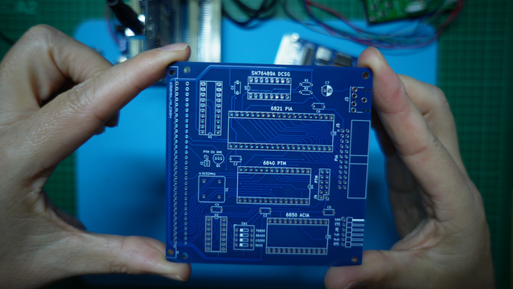
The PCB looks great! So, let’s get our first one assembled.
For assembly, I started off with the bypass capacitors, and the two resistors.
Then I soldered in the IC sockets, including the 8-pin IC socket that I’d modified for the Crystal Oscillator, as I explained in earlier posts.
I then also soldered in the TO92 MOSFET and the 2 pin header for the Timer’s optional NMI connection.
Then, the 3.5mm audio connector, the right-angle header for the TTL serial interface, and the audio output electrolytic capacitor.
Then, the 4-way Dual In-Line switch for baud rate selection.
Then, the two I/O IDC connectors.
Finally, the male DIN 41612 MECB bus connector, which is secured in place with a couple of 10mm M2.5 bolts.
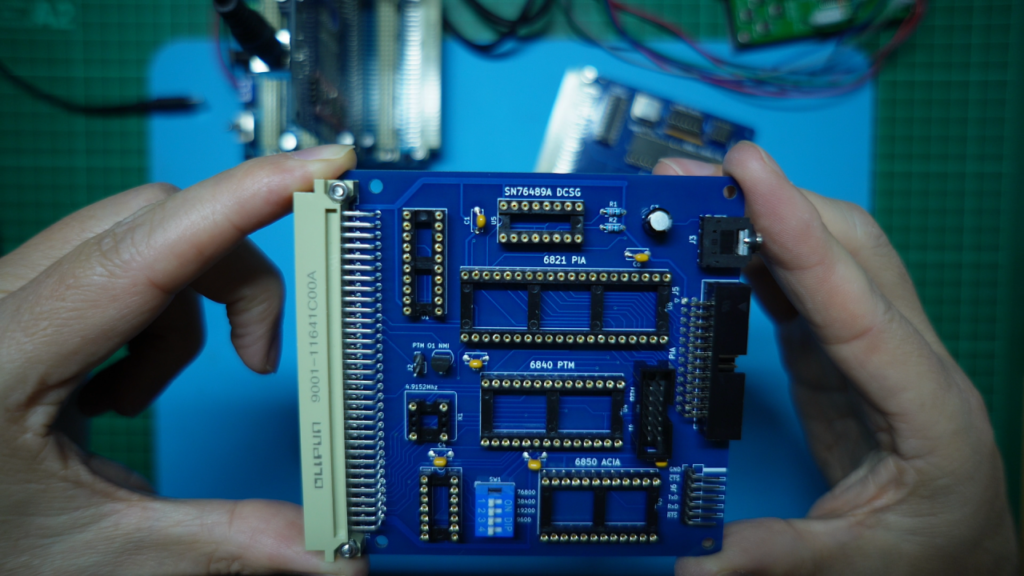
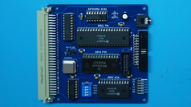
With the board assembly completed, it was time to get some IC’s inserted.
I started with the 74HCT393 Baud Rate divider.
Then, the three Motorola Peripheral chips. The SN76489 Sound Generator, and the 4.9152Mhz Crystal Oscillator.
Finally, I needed to program a PLD for the desired addresses assigned to the Peripheral chips.
As I’ll initially utilise the same ASSIST09 monitor that I was using on my 1980’s Wire-Wrap 6809 card, I define the I/O Address space on the CPU Card as E000 – E0FF.
The three Motorola peripheral IC’s are allocated an 8 byte address space each, starting at the I/O addresses 00, 08, and 10.
So this gives us the following device addresses:
- MC6840 PTM = E000
- MC6850 ACIA = E008
- MC6821 PIA = E010
This Chip Select address assignment is then setup in the PLD.
If you want to know more about the Minimalist Europe Card Bus use and programming (of the ATF16V8 PLD), then I recommend viewing my earlier post / video covering the MECB Address Decode / Glue Logic.
Here is our WinCUPL definition for our I/O Card PLD.


In the WinCUPL source you’ll first see the standard header and the Input pin assignments.
Then, in the second page of the source you can see the three standard chip select output pin assignments for CS1, CS2, and CS3.
These are all as per the standard PLD usage, that I originally defined for my Minimalist Europe Card Bus peripheral cards.
Finally, at the bottom of the source, there is the three lines of logic equations which define the chip select output logic.
Pretty straight-forward!
I then used WinCUPL to compile that source file into the required .JED file, for programming the PLD chip via my TL866 programmer.
Once the PLD was programmed, I then inserted it into our I/O card.
As mentioned earlier, for an initial test I’m using the same Motorola ASSIST09 Monitor that I was using in my original 80’s wire-wrap CPU card.
This will test both the ACIA and PTM peripheral chip’s operation, as both are used by the ASSIST09 monitor.
For this test I also installed the NMI jumper, to enable the PTM output to trigger a Non-Maskable Interrupt of the CPU.
Next, I program the original 2KB ASSIST09 monitor code into the top 2KB of a 28C256 FLASH ROM.
This ASSIST09 ROM was then installed into our 6809 CPU Card, replacing the ROM which held the TMS9929 Video Card test we had used in a previous post / video.
Finally, I checked that the CPU card DIL Switch was correctly set for the I/O Address space allocation of E000 – E0FF.
It was already set for this I/O Address space, as we’d used this same I/O address block for the TMS9929 Video Card, which was allocated an 8 byte I/O space starting at I/O Address 80, so effectively at memory address E080.
This address allocation also means that I can just use the existing Video Card alongside our new I/O Card, without any configuration changes being necessary (to avoid any address space allocation conflicts).
So with that all done, we were then ready for our first Motorola I/O Card test!
For the test, I first connected up the I/O Card’s TTL serial port to a TTL to USB adapter and then plugged in and also ran Tera Term on my PC.
With that sorted out, I then inserted the CPU Card and I/O Card into our backplane, alongside the existing Video Card.
Then, it was time to apply power and see what happened.
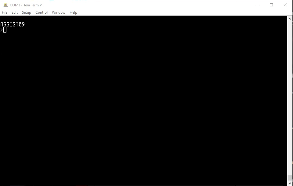
We got the ASSIST09 prompt, so we know the ACIA is working.
To test the PTM and the NMI Interrupt driver, we can verify that the breakpoint and single stepping functionality of ASSIST09 is working correctly.
To test this, I used the simple “Hello World” program that I demonstrated in an earlier post / video, which covered firing-up my old 80’s wire-wrap homebrew 6809 board. You’ll find that post here.
This earlier post / video also demonstrated both the operation and the available commands of the ASSIST09 monitor, so I won’t repeat that here.
So, I first issue the L (Load) command to ASSIST09. Then I used the Tera Term “Send File” option to send the assembled “Hello World” .S19 file to our CPU card.
This short program was assembled targeting memory location 0000, so by displaying memory address 0000 to 001F D 0 1F, we can see the program is present.
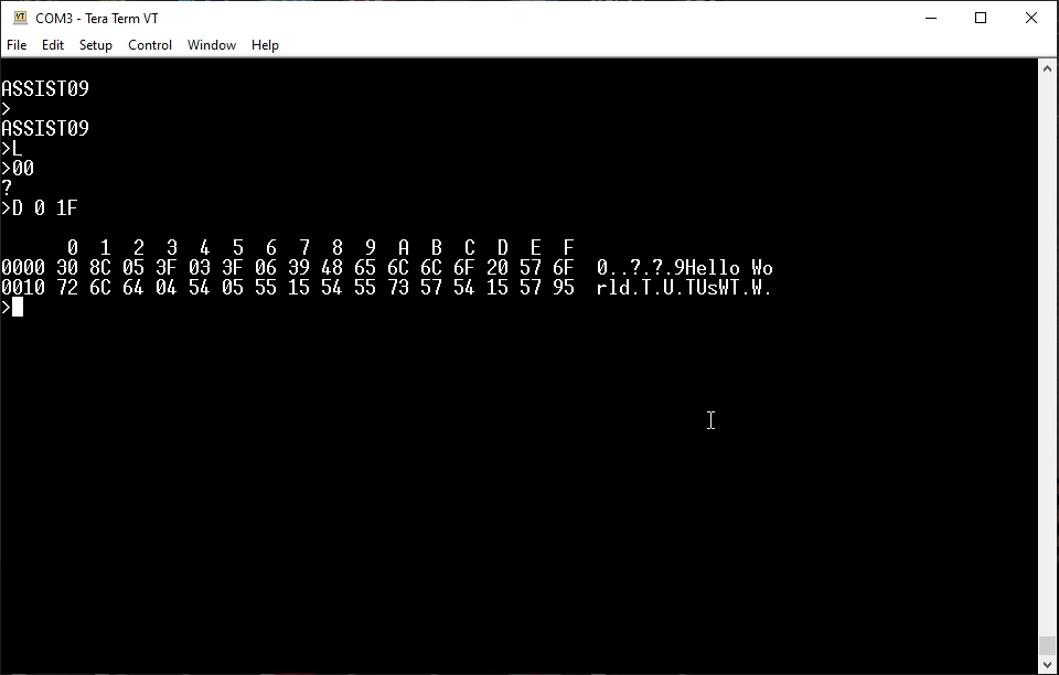
Calling the program with C 0, we can see the program run and display the expected “Hello World”.

Now, to first test that Breakpoints are working.
First I set a breakpoint for address 0000, so our program should immediately stop before executing the first instruction.
So, B 0
Then if we call the program again, with C 0, we see our breakpoint has worked. We have stopped with the Program Counter at 0000.

Now I set the Stack Trace level to the current Stack Pointer value, using the S command.
Then we try a single step using the period (.) command.
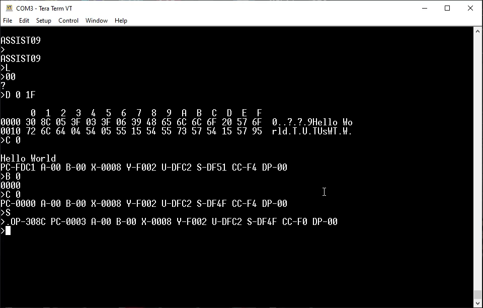
And we are looking good. The program counter is now pointing at address 0003, which is the second instruction.
The first instruction’s opcode (OP) was 308C followed by the 7 bit Offset Operand 05, which loaded the X register with the effective address of our “Hello World” string, being a Program Counter offset of 5, which is at address 0008 (PC = 0003 + offset of 05).
And, we can single step the rest of the program withe repeated . until we return from subroutine to the monitor (Opcode 39 – RTS).

So, Breakpoints and Single Stepping are verified working!
We’ve now verified our ACIA, PTM, and NMI Interrupt driver are all successfully working.
This just leaves our PIA and Sound Generator chips, which I’ll need to write some code in order to test.
For now, I think we’ll call it for today, with our Motorola I/O Card looking like a success.
At least, I now have a modular Minimalist Europe Card Bus (MECB) based 6809 system that updates my original 80’s wire-wrap card, with a fully configurable memory map. As currently configured, I have a full 56KB of RAM, a TMS9929 Video Card, and (subject to final testing), a PIA with a Sound Generator to complete a nice little retro 8-bit system.
Next, I might explore a different CPU card…
I’m gonna have to go back and learn all about how interrupts work – I should be able to wire up a keyboard pcb to an Arduino or Pi-Pico to tickle interrupts through this as a keyboard of sorts, right?
Perhaps this old dog isn’t learning quite like he used to…
😛
It depends on your target platform. For our retro 8-bit projects, interfacing a keyboard through a MC6821 PIA (for example), allows you to trigger a CPU interrupt (IRQ) via a PIA Port control input.
e.g. On the DREAM 6800 Hex Keypad matrix interface (schematic shown in my Hex Keypad – Part 1 post), a quad input NAND gate is used to trigger a rising edge on the CA1 input when a key is pressed. This subsequently triggers a CPU interrupt.
Likewise, if you were using an ASCII Keyboard encoder chip (or an MCU / Arduino), to feed in a parallel ASCII code into a PIA port, the keyboard encoder’s Strobe signal could trigger CA1.
Then you just need to write an Interrupt Service Routine to retrieve the key code and store it in a key buffer (for your mainline application to action), and then Return from the Interrupt (e.g. RTI).
Depending on your system, you either first call a monitor routine to register your new Interrupt Service Routine, or (if writing your own monitor / system), you’d set the CPU’s IRQ Interrupt Vector to point to your Interrupt Service Routine in ROM.
…(casual whistling)
soooooo….. how fast d’you reckon that Z80 CPU card will clock out at?
(more casual whistling)…
Good question. I’ve just finished testing the 6809 system at it’s full rated ‘B’ version 2Mhz system clock.
For a Z80 CPU card, I’d probably first test the system with the early 4Mhz clock speed (my existing Z80 chips are from the 80’s), then ramp it up from there.
Although, many Z80 systems from the early 80’s period were clocked at the color burst frequency of 3.5795Mhz. So, if intending to replicate some early systems, then higher clock speeds may not be necessary (or desired).
Of course, for a Z80 system I’d also need an appropriate I/O card to go with it. Lots to do. Lots of fun! 🙂
On that, say by chance I had ordered a handful of 68C09P and 68C09EP microprocessors, would clocking to 3Mhz (or perhaps a little higher) be too far out of the question… for purely experimental reasons, of course…?
I think you might have meant the Hitachi 63C09? Motorola 6809’s only went up to 2Mhz (MC68B09).
I’m not sure if I have any HD63C09 3Mhz CPU’s in my stock. I’ll have to check.
I’d also need a 12Mhz oscillator to give them a try at the 3Mhz system speed.
Then there is the question of whether the Motorola ‘B’ speed grade peripheral chips (on my existing Motorola I/O card), will work if pushed to 3Mhz, or whether a different I/O card would be needed (e.g. based on WDC 65Cxx peripheral chips)?
I’ll probably give 3Mhz a try, but first I’ll have to see if I have the necessary parts (a 63C09 and 12Mhz oscillator).
Yes – you are correct, I did mean 63C09 – perhaps a speed challenge video might be another video you could try after you’ve sorted the 3(+) CPU & I/O cards & run out of other things to do? I imagine there’s no issues with my clocking them at lower speeds in the mean time…
Well, I found I have some HD63C09 CPUs in-stock. They were put aside as they are HD63C09E (external clock) chips mis-marked as HD63C09P.
But, as I now have my updated v2.2 6809 CPU card (which takes either internal or external clock CPU’s), my system is now happily running a HD63C09E processor.
Although, currently it’s still running at 2Mhz, as I don’t have a 12Mhz crystal oscillator in-stock.
So, I’ve now added a 12Mhz oscillator to my next parts order. When that arrives I can do a 3Mhz system test, and also see if the Motorola I/O card will operate exceeding its 2Mhz ‘B’ chip rating.
Yes, I have a number of new cards on my next to-do list. Plenty to do!
Awesome!! I’ve looked at getting some cards, but am I right in thinking that there’s only the backplane card available right now? I thought I might be fancy and have a go at kicad to draw up something to suit my condensed backplane idea too, but that’s yet another whole new level of learning I have to go through again. Given I have no idea what I’m doing, I guess I’ll stand by to stand by…
Well, I’ve only managed to list the backplane on my Tindie store, so far. It was the logical card to start with. I just need time to get more of the completed cards listed.
I’m also not sure yet how I should list them. I’m thinking I might just get the PCB’s listed, with just a few component pack options for the more unique parts (like the DIN connectors), instead of full kitsets of parts.
Not sure yet. I have plenty of parts in stock, but assembling full kitsets might be pretty time consuming, and many enthusiasts have probably already got many of the components needed in their own parts drawers?
What do you think? You definately should have a play with KiCAD. It’s a learning curve, but also a lot of fun.
You’re right, I’ve been putting together a few electronic kits off Tindie, and imho this would be the exact market demographic for your projects/kits too – I have a few items I’ve recovered from old printers and photocopiers, like a couple of backplane connectors (though my vertical backplane DIN connectors have all three rows of pins on them, so I’d still have use for 2 row connectors as well as all the corresponding daughter board connectors too), so perhaps both a BOM for filling out our own parts, and a selection of items/kits would indeed be the go – building things until I learn to design my own, will scratch that itch in the mean time!
I’ve had some free time without family and have crammed some pretty good time in on learning some new stuff – FreeCAD and KiCAD being the latest – it’ll be a long road tho!! -_-
Yes, I’m working on properly documenting the BOMs. So, I think for Tindie I’ll go with PCB’s with various component pack options.
Depending on the item, the option packs may make up a full kit (eg. Like the existing Backplane listing), or they may only make up to a short-form kit.
A CPU Card is a good example, where different people might want different CPU’s or clock speeds, so probably best to leave the CPU and Crystal Oscillator choice up to the individual.
But I might offer a programmed ASSIST09 ROM and a programmed default memory-map PLD as options, for those who don’t have a programmer and just want to get up and running quickly.
As regards FreeCAD and KiCAD, I took the route of deciding first which EDM tool is most likely to fulfill all of my longer term needs, so that I could focus all of my efforts on just learning the one tool.
Of course, with any new tool, it’s just a matter of getting plenty of real hands-on experience, to become proficient in it. So, I believe just diving straight in and working on a design you want is the best way to go.
Love it! Especially since I’ve started collecting items myself already – and keen to work out a backplane solution that will work with this standard too – that save my having to know what I’m doing to have a viable pool of applicable hardware, cards and software to go with it.
I’ve been meaning to get into some form of CAD for my 3D printing and CNC work, and electronic PCB design for all these side projects I’d like to get into, so FreeCAD and KiCAD seem to be the go, so much of my spare time away from the family has been sunk into youtube videos and as you say, “hands on” with the apps themselves…
It’ll be a while, but confident I’ll get there…