
Continuing on, with my Minimalist Europe Card Bus project.
Join me as I introduce a 1MB ROM Expansion Card, discuss the design decisions, and assemble my first card.
First some background.
Some time ago, I decided I wanted a “Cartridge” style ROM Card, to plug into my MECB backplane.
This thought originally came about, while considering that I might eventually mimic the CreatiVision TV console, of the early 1980’s.
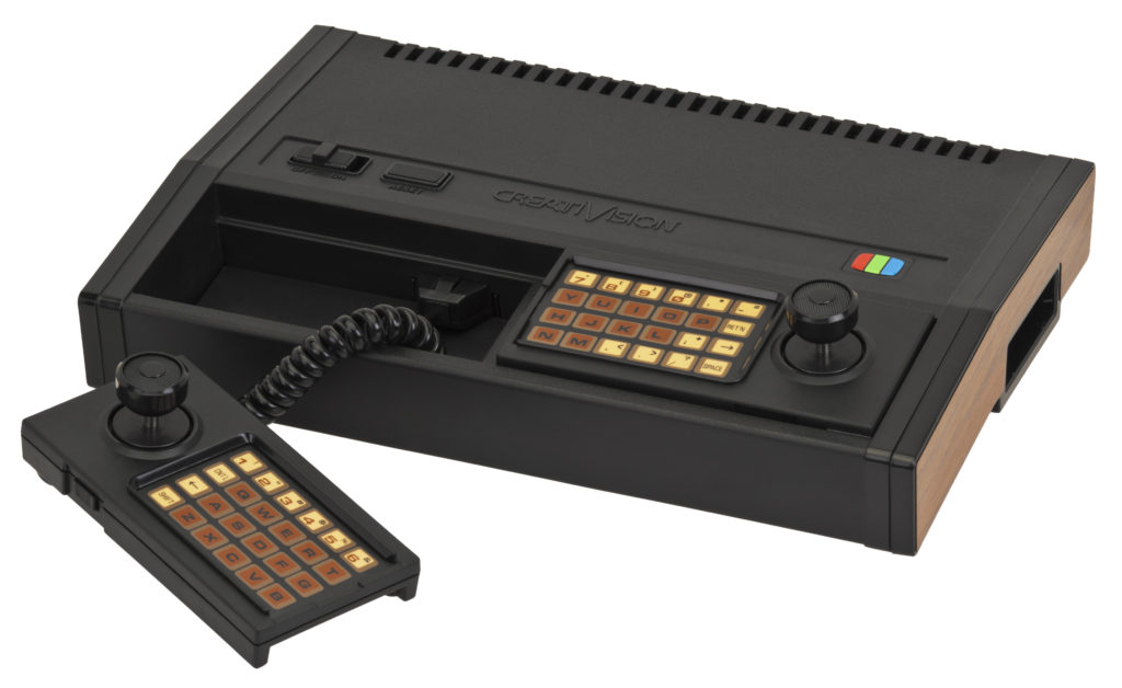
The CreatiVision was a 6502 based system, which also used the TMS VDP Video chip and a Motorola PIA.
So, once I have a 6502 CPU Card, to team up with my existing TMS9929A Video Card, and Motorola I/O Card, I’ll be ready to explore this possibility.
Some form of game controller, or keyboard, will also need to be devised.
Originally, I was thinking of just using a Backplane Card slot, as a custom “Cartridge” slot, for inserting pre-programmed ROM Game Cartridges, similar to the original Game Console cartridge experience.
But, after expanding on this idea, and after checking what appropriate Dual Inline Package ROM chips were available, at a reasonable price, I arrived at the thought of instead making a bank selectable 1MB ROM Expansion Card.
In this way, one card could be used to hold maybe 16 games, each selectable via a bank select switch, for a TV Console recreation.
In addition, the ROM Expansion could be used with any CPU Card, to allow easily switching ROM images, each mapped within an 8-bit CPU’s 64K address space.
It also further occurred to me that the original 64-pin ECB bus, actually had 20 pins allocated for the Address Bus, on the original 64-pin ECB A&C rows.
That is, A0 – A19, allowing a full 1MB to be addressed from the existing MECB bus.
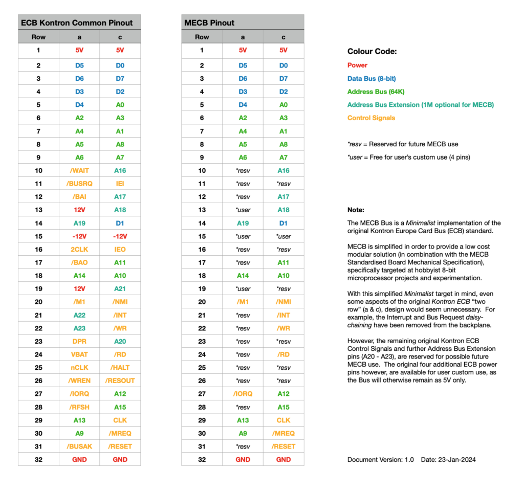
As a result, I’ve designed a flexible 1MB ROM Expansion Card, that will combine a manually switchable ROM bank (for CPU Cards that only support the A0 – A15 64K memory space), with the ability to (instead) configure support for utilising the additional A16 – A19 address bus pins.
Effectively, allowing the full 1MB to be addressable from the MECB bus.
This flexibility, will be useful for potential future CPU Card designs, that can address a full 1MB A0 – A19 address space.
For typical 64K addressing 8-bit processors, this would be implemented via some form of Memory Management Unit (MMU), located on the CPU Card, to provide the additional 4 address lines, beyond the normal A0 – A15 64K address space.
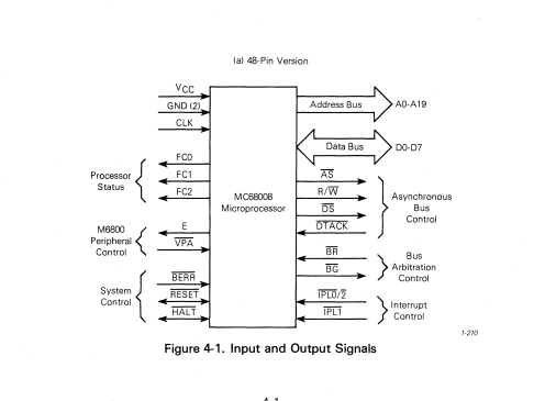
Alternatively, more advanced 8-bit data bus CPUs, like the Motorola 68008 (in it’s DIP48 package), natively provide a 20-bit address bus, capable of addressing a full 1MB of linear address space.
To provide this flexibility, a PLD will be used to configure between manual 64K block selection, or, the use of the full 20bit address bus.
Also, as with other MECB Cards, the PLD will also allow flexible configuration of the Card’s address space use.
This could either be the address space allocated within a 64K bank, or, the overall address space allocation within a full 20-bit 1MB address space.
In effect, the bus A16 – A19 address lines could be selected to address the 1MB ROM space, or, the manual 64K bank switch control is used to select 1 of 16 possible 64KB blocks, which is mapped into the card’s PLD configured ROM address space use.
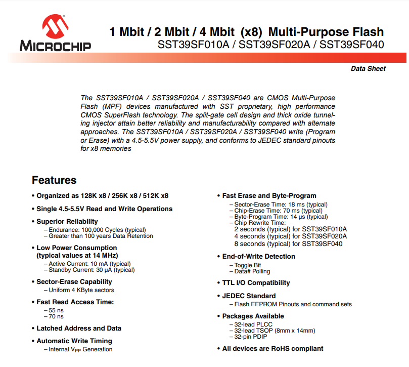
Finally, to satisfy low cost and Retro friendly Dual Inline Package ROM chips, I’ve chosen the SST39SF040 32-pin 512KB Flash EEPROM chips. In this way, you can also choose to only populate one ROM chip, if you only require 512KB (or 8 possible ROM banks).
So, with that background and detailed overview, let’s now take a look at the schematic.
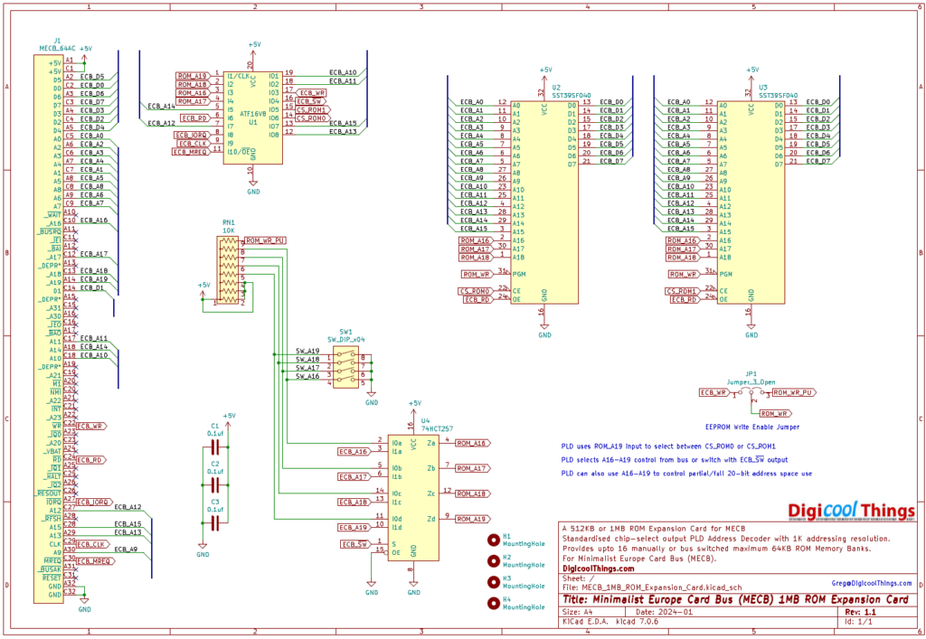
As can be seen, we have our two 512KB Flash ROM chips allowing for 1MB of storage.
We also, have our usual PLD chip, however for this card the lower 5 address lines, normally used for allocating I/O address space usage, have been repurposed with the high 4 address lines A16-A19, and the addition of A10, to allow a more granular 1K boundary within the 64K address space.
So, we effectively have the full A10 – A19 address lines available to the PLD, for the card’s address space allocation.
Finally, we have a 74HCT257 quad two input multiplexer, to allow the PLD to also select whether the A16-A19 address lines originate from the bus, or, from our 4-way manual bank select switches.
And that’s pretty much it. We also have a jumper, to control connection of the Write signal to the ROMs, or whether to just treat them as Read Only.
So, let’s now have a look at the PCB layout.
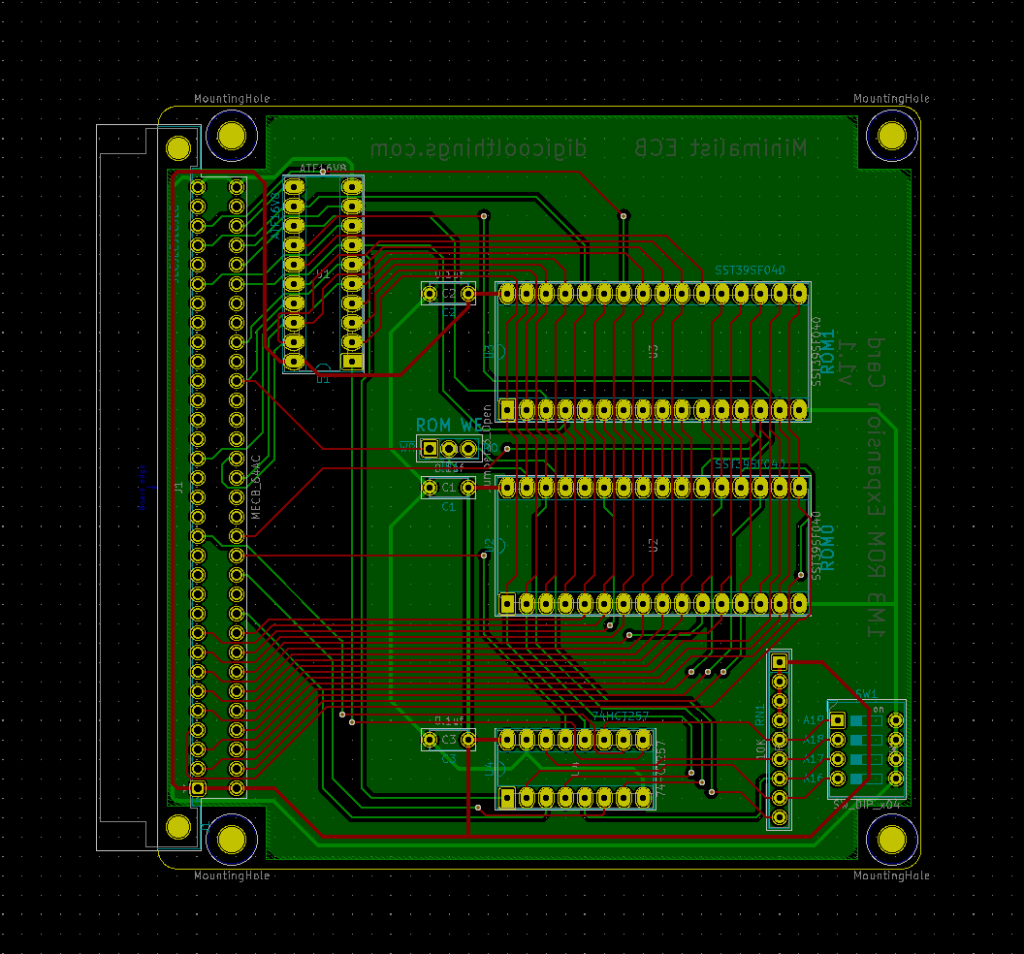
The PCB layout is pretty straight-forward, again, with the starting point being the MECB KiCAD template, that I created earlier.
Note, that I’ve positioned the bank select switch at the top edge of the board, for easy access.
The silk-screen identifies ROM0 and ROM1, to easily differentiate the two 512KB ROM chips.
The bank select switch footprint is a normal 4-way DIL switch, in a DIP8 package.
You can, of course, just use a 4-way DIL switch, but the DIP8 footprint also accommodates a rotary coded switch, which allows a very easy 1-of-16 bank selection, without needing to toggle four binary switches.
I’ve used rotary coded switches for other projects, and quite like them.
However, a warning regarding where you source these from!
I found a good price for some 16-way switches on AliExpress, and because of shipping cost (and that I use them in other projects), I ordered a larger quantity from the AliExpress supplier.
What a mistake! They appeared okay on receipt, however, when I went to use them, the legs just break-off, when trying to insert them in the PCB.
Here’s an example.
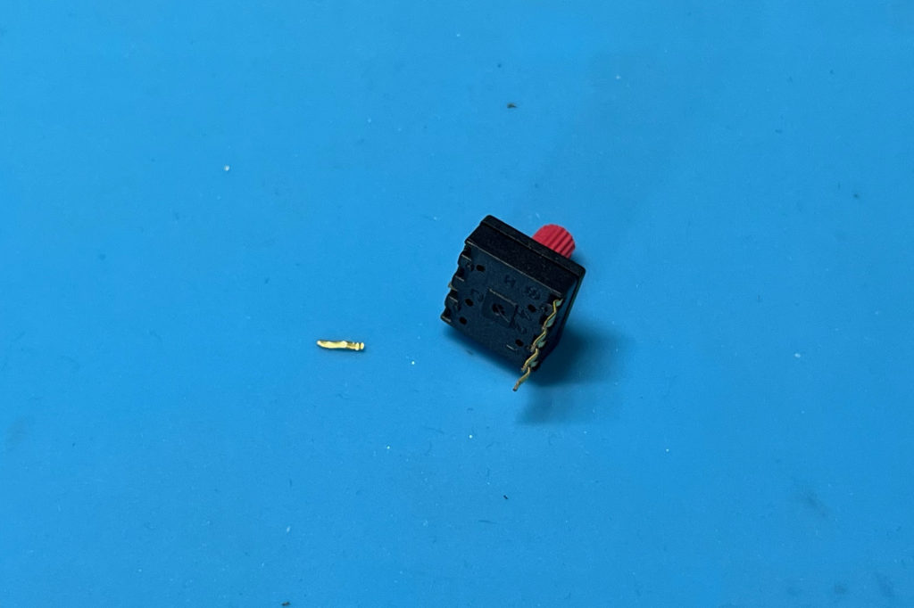
The pins seem to be made of an incredibly low quality metal, that just breaks, on the first sign of even slight bending.
This also raises the question, of whether the rated 20,000 switch operations, is believable.
This was unfortunately a quite costly mistake, and since I didn’t discover this quality issue until over 14 days after receipt, I had no recourse via AliExpress, and I couldn’t even post a review to warn others.
So, please be warned!
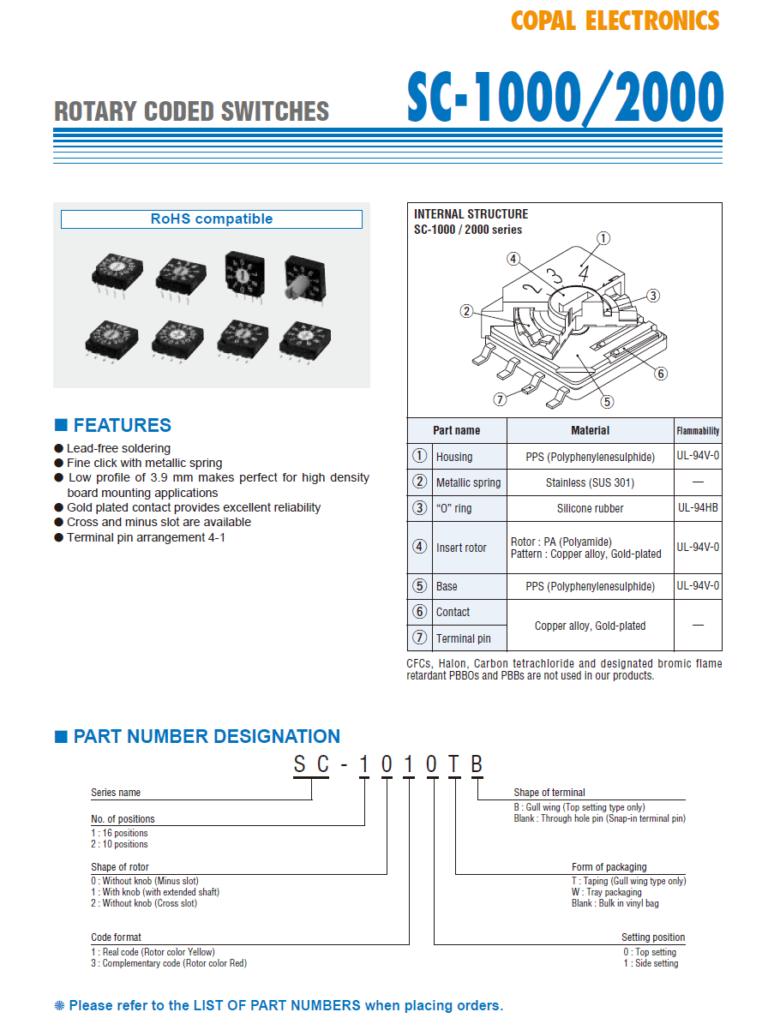
I only recommend using genuine Nidec Copal Electronics rotary coded switches. For this project, specifically the SC-1130. These are much more expensive, but I have used them for years, and they are genuinely good quality.
Of course, you could just use a simple 4-way DIL switch!
So, with that covered, let’s get our first 1MB ROM Expansion Card assembled.
I started with the IC sockets. 2x 32-pin, a 20-pin, and a 16-pin.
Next, the 3-pin Jumper header, and the bypass capacitors.
Then, the Single Inline resistor pack.
Then, the right-angle male DIN 41612 bus connector, which is held in place with two 8mm M2.5 bolts.
Finally, I soldered in my Nidec Copal SC-1130 Rotary Coded Switch.
With the PCB assembled, I’ll next insert the 74HCT257 quad two input multiplexer, and a jumper in the Read Only position.
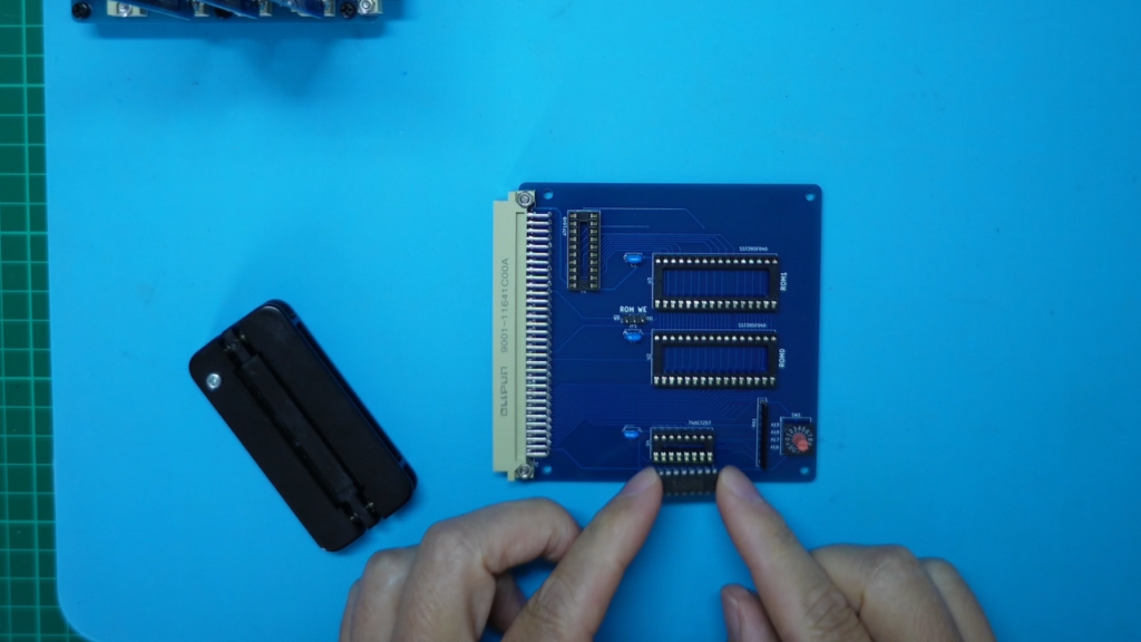
This just leaves the PLD and the ROMs, which we need to configure, depending on how we intend to use the ROM Expansion card.
But, at this point I’ll leave this for Part 2.
I think this intro, design presentation, and first Card assembly, is probably enough for this video.
So, until then…