
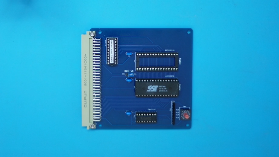
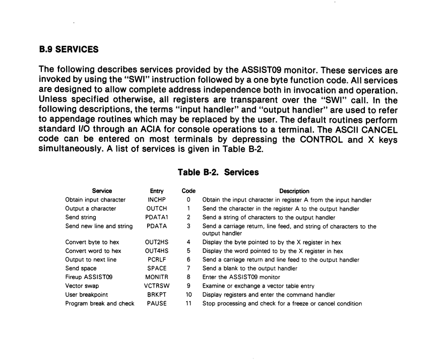
With our 1MB ROM Expansion Card design and assembly already presented in Part 1, it’s now time to test our assembled Card, with an initial use scenario.
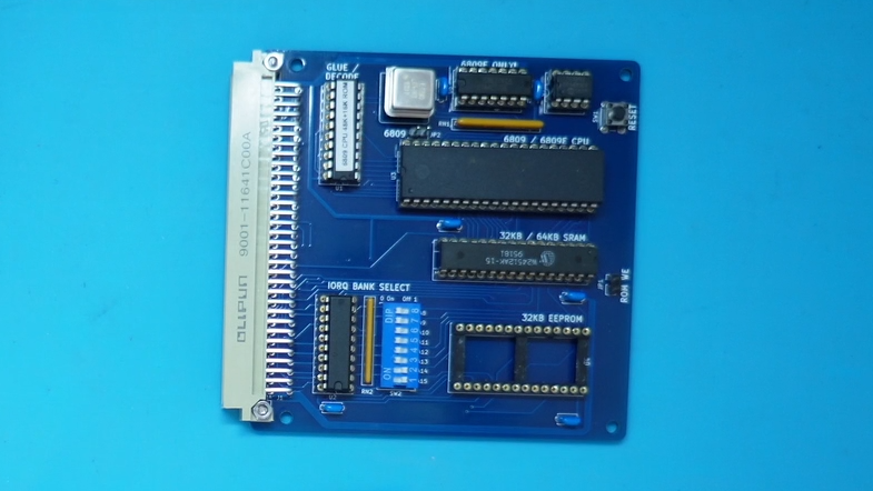
Initially, I’m going to use the ROM Expansion Card with my existing 6809 CPU Card.
So, we’ll need to configure and program, a PLD chip and a ROM chip, for our intended Memory Map and Card usage.
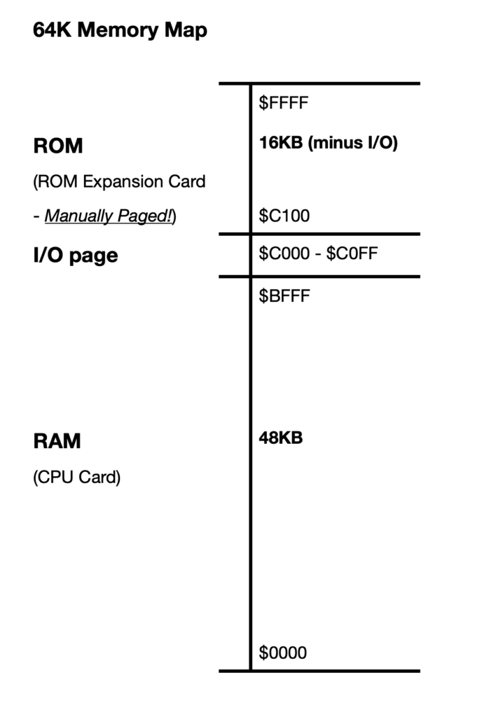
For this exercise, I’m going to configure the CPU card PLD for RAM allocated to the bottom 48KB of the 64K address space. i.e. $0000 to $BFFF.
I’ll also configure the CPU Card’s Dual-Inline switch, for the I/O page allocation to be at the bottom of the expanded ROM space.
i.e. Memory page $C0. Therefore, I/O will use the address space $C000 – $C0FF
Then, for our new ROM Expansion Card, I’ll configure the PLD to enable manually switched 64K bank selection, with the allocated ROM space being in just the top 16KB of the 64K address space.
i.e. $C000 to $FFFF.
So, here’s the WinCUPL pin logic source code for the 6809 CPU Card PLD.
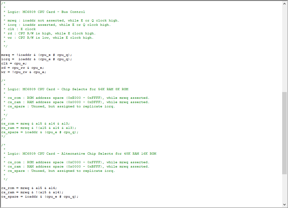
As you can see the logic is very simple. Only address lines A14 & A15 are needed to determine the bottom 48K for the RAM chip select.
Next, here is the WinCUPL pin logic source code for the ROM Expansion Card PLD.
Again, very straightforward, with only A14 & A15 address lines required to determine the upper 16KB of the 64K address space, allocated for ROM.
Note also, that A19 is used to select between the two possible 512KB ROM chips, ROM0 and ROM1.
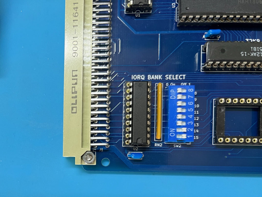
Finally, the A16 – A19 address line source for the ROM is set to be from the manual bank select switch (low level), instead of from the MECB extended address bus.
You might also note, I’ve added a configuration (currently commented-out), for a top 32K ROM bank (instead of 16K). This seemed another likely memory map scenario, for implementing a ROM based system.
For testing the 16K ROM configuration, I’ll start-off with the first two banks of the ROM containing, firstly, the ASSIST09 monitor, and secondly, the Extended BASIC interpreter. Both of which have been presented in previous blog entries / videos.
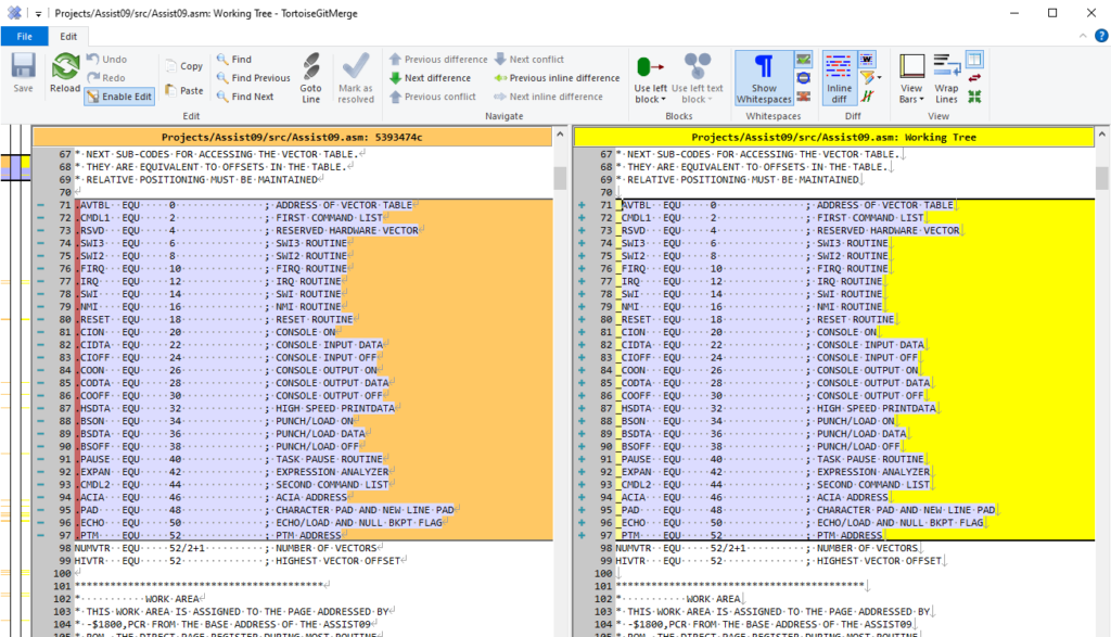
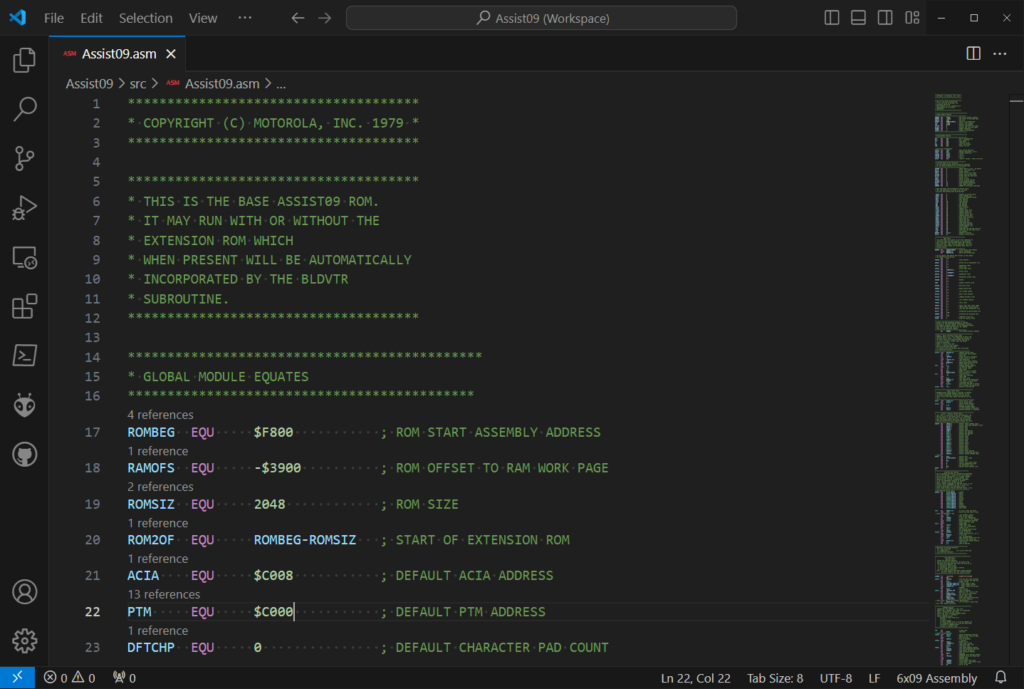
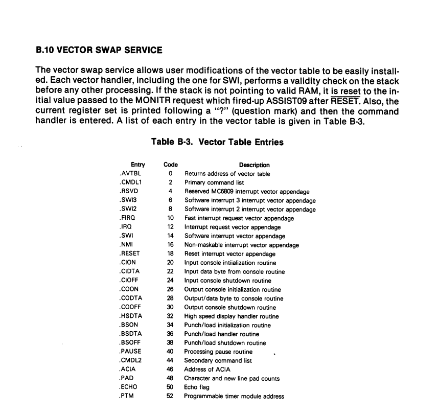
For ASSIST09, I’ll first need to make a change, to identify that the top of RAM is now at $BFFF (instead of the original $DFFF).
Also, we need to change the PTM and ACIA I/O addresses, to their new positions of $C000 and $C008, respectively.
With this configuration, I’ll be able to swap between the ROM code configurations with just a click of the bank select switch.
This also leaves up-to 14 unused ROM banks, for future use.
Now, to reliably make these changes, to our ASSIST09 ROM image, I should re-Assemble from some altered Assembly source.
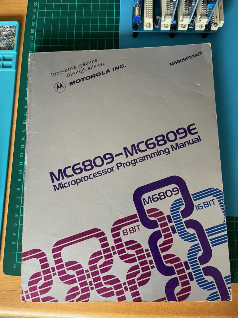
Interestingly, my own ASSIST09 ROM binary image, actually originates from when I manually keyed in the 2K of Hex code, as obtained from the ASSIST09 Assembly listing in my original Motorola MC6809 Microprocessor Programming Manual. This was way back in the early 1980’s!
In fact, I don’t recall ever Assembling ASSIST09 from the source code!
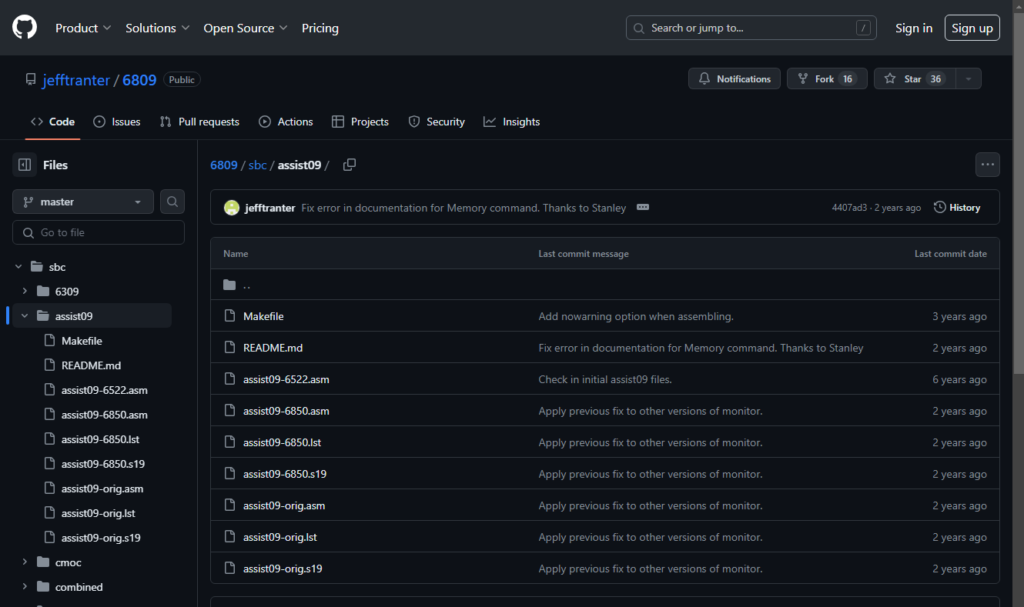
So, I found some ASSIST09 source code on Jeff Tranter’s 6809 GitHub repository.
Specifically, the file assist09-orig.asm seemed a likely candidate.
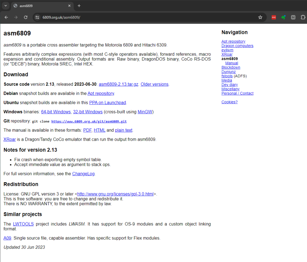
The first step was making any changes necessary, to allow assembling with the ASM6809 assembler that I was currently using.
As each line’s comments were already prefixed with a semi-colon, it turned out that the only change required was changing the . prefixed labels, to instead use an under-score _ prefix.
The only other issue stopping successful assembly, was the occurrence of a CPX instruction.
I checked with my original Motorola 6809 guide manual, and this error (if it was an error?), was also present in the original listing.
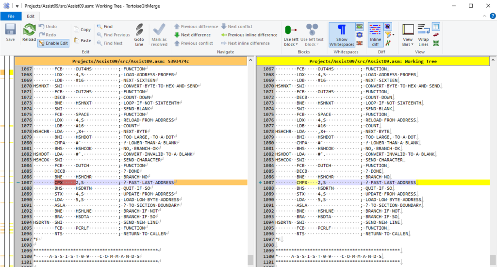
It’s interesting as the CPX instruction mnemonic exists for the earlier MC6800 processor. But for the MC6809 the equivalent is the CMPX instruction.
So, with this minor edit completed, I had a successful assembly.
The next step was to “file-compare” the binary output of the Assembly, with my known-good original ROM binary image.
This highlighted several differences (perhaps typos?), in the ASSIST09 source file I had obtained.
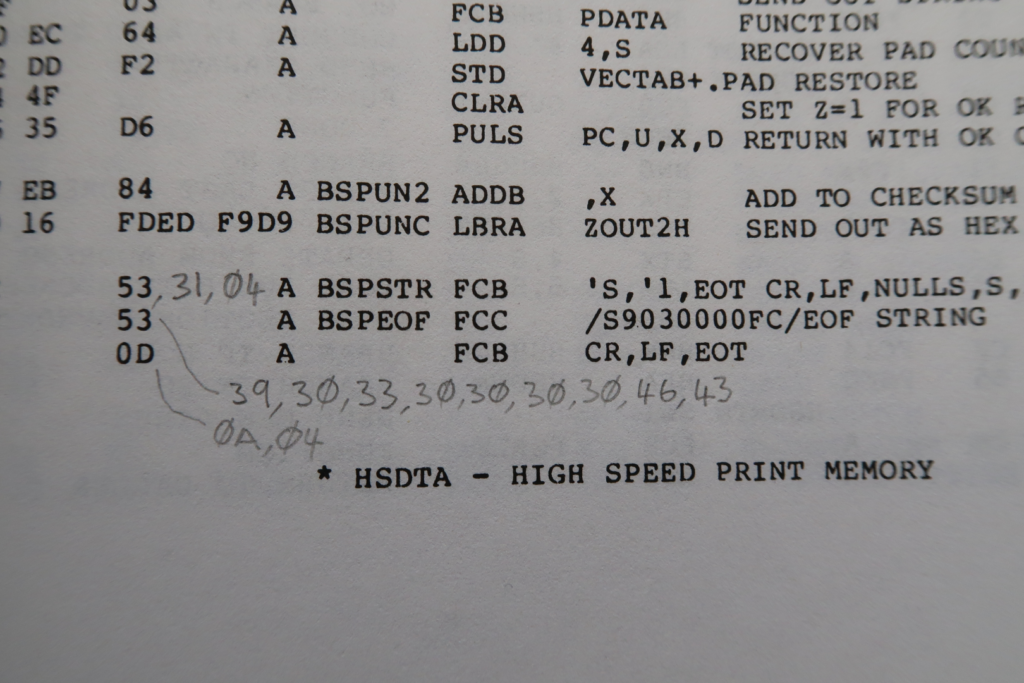
Cross-referencing these with the official Motorola 6809 Microprocessor Programming Manual, confirmed the so called “original” source file was indeed incorrect.
Several incorrect instructions were located in the Character Output subroutine CODTA
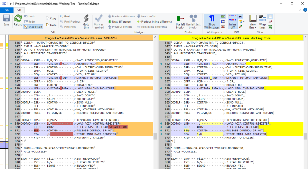
Also, an ASCII ‘1’ had been entered as Hex 1 (no single-quote prefix), therefore not creating the correct ASCII code for the 1 character (i.e. Hex 31).
With these corrections made to the Assembly source code, I was finally assembling an identical bin file output, when compared to my original 1980’s hand entered hex ROM image!
I will be sure to add this to the MECB Github repository, so that a genuine “original” ASSIST09 source file, that can be assembled with ASM6809, is available for others to experiment with.
With the corrected original ASSIST09 source, I can now make the simple changes required, for my ROM Expansion Card’s first test.
As noted earlier, all I need to do is change the RAM workspace offset from -1900, to instead be -3900. This shifts the top of RAM workspace from the $DF00 page to $BF00.
Also, change the PTM and ACIA device addresses from $E000 and $E008, to instead be $C000 and $C008, respectively.
Next, we need to also check / change the Extended Basic source code. Again, for the ACIA address of $C008.
With these changes made, we can assemble the source to Intel hex code files, ready for the ROM programmer.
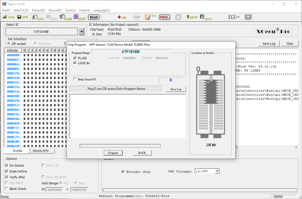
So next I program a SST39SF040 512KB ROM chip, with these two hex code files loaded into the first two 64KB banks.
Firstly, I load the ASSIST09 file into the first 64K bank of the ROM. So that’s bank 0.
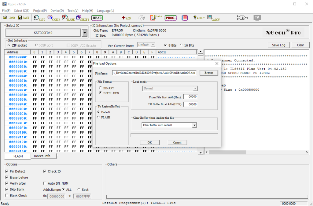
I then load the Extended Basic file into the second 64K bank of the ROM, by specifying to load the file at offset 1-00-00, and selecting to, not clear, the ROM programmer’s buffer.
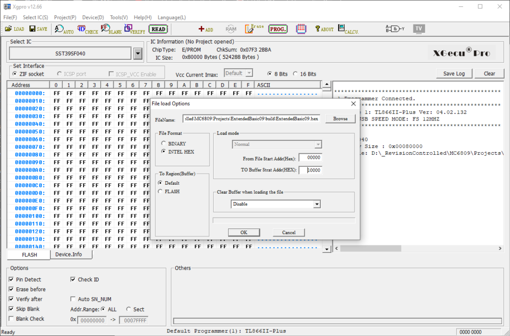
With both banks 0 and 1 loaded, I then program this into the ROM.
And with this, our ROM0 is ready to go.
With the ROM programmed, I now program two PLD chips with the code that I showed earlier.
Firstly, the PLD for the CPU card.
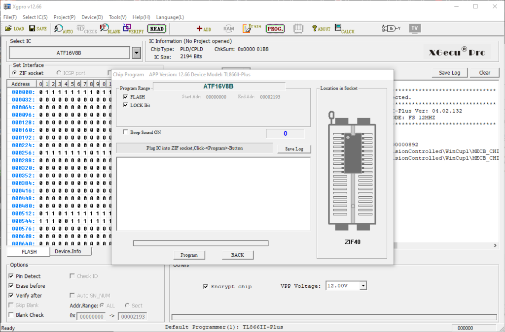
Then, the PLD for the new ROM Expansion card.
With that done, it was time to get the programmed chips inserted.
The SST39SF040 goes into the ROM0 socket.
Then, I insert the ROM Expansion card PLD.
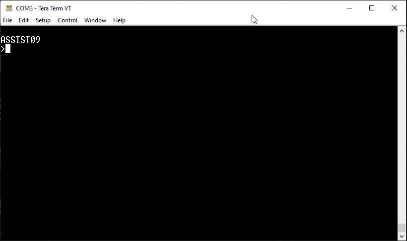
With the bank switch initially set to bank zero, if all goes to plan, we should initially boot up with ASSIST09.
For the CPU card, I also insert the updated PLD chip.
Then, I changed the I/O bank select DIL switch to be bank $C0. Therefore, just the A14 & A15 switches are set to 1, with the other 6 address lines set to 0.
Finally, I remove the CPU Card’s on-board ROM chip, as we’ll now be running the ROM code from the new ROM Expansion Card
Okay, we’re now ready for our initial test, to see if we still boot-up with ASSIST09 executing from the new ROM Expansion card.
Okay, that didn’t work! So, time for a little debugging.
First, I tried dropping the Crystal Oscillator frequency from 16Mhz to 8Mhz, so that I was running the system at the rated clock speed of the MC68B09 CPU, which I currently have inserted.
Again, No joy. 🙁
Next, I went back and programmed the updated ASSIST09 code into my CPU Card’s 28C256 32Kx8 ROM, and inserted it back into the CPU Card.
This was to check whether all was working, without the new ROM Expansion Card in use.
This time we had Success!
So this effectively confirmed the issue was with the new ROM Expansion card, as opposed to a ROM code error.
With the ROM code confirmed, next step was to re-look at the PLD logic.
And… this is where the error in my logic became immediately apparent!
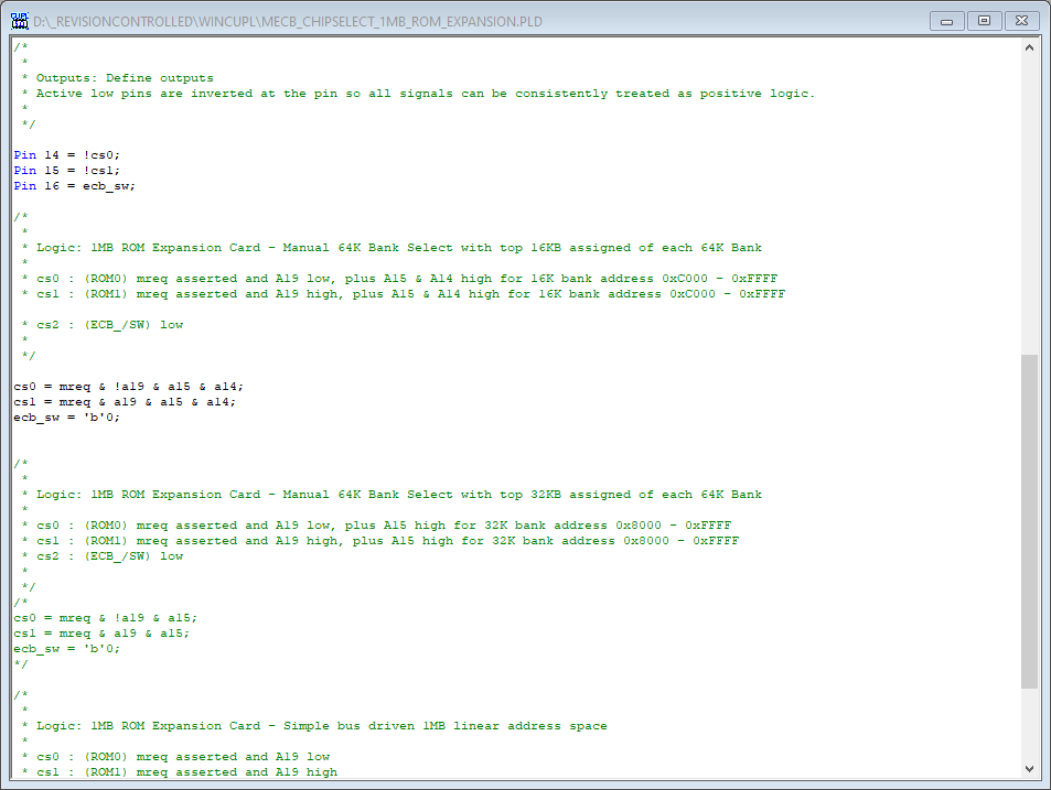
To ensure the logic equations are easy to read (by consistently using positive logic), I invert the negative logic signals at the pin definitions. Chip Selects are traditionally negative logic (active low), so my three possible Chip Select outputs are negated at the output pin definitions.
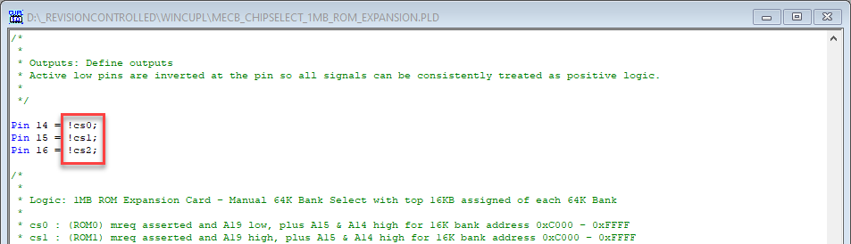
This is where I made my logic error. Chip Select 2 (i.e. cs2) output, is being used to select the A or B input of the 74HCT257 Quad 2-line to 1-line Multiplexers.
In error, I’d simply set the high or low level, based on the 74HCT257 data sheet, overlooking the fact that I was inverting the signal at the output pin!
The solution to this is to remove the signal inversion, at the output pin definition.
For clarity, I also renamed the pin so that its use is no longer confused by the Chip Select terminology.
So, with that correction done, I reprogrammed the PLD and re-inserted it into the ROM Expansion Card, ready to try again.
Feeling confident, I also returned to the 16MHz CPU Card crystal oscillator, so that I’m once again double-overclocking my Motorola MC68B09 to run at 4MHz (instead of it’s maximum rated 2MHz).
Yes! This time we have ROM Expansion Card success! Good so far. 🙂
So, then for the final test. I turn the system off, and switch to the second ROM bank, and once again apply power…
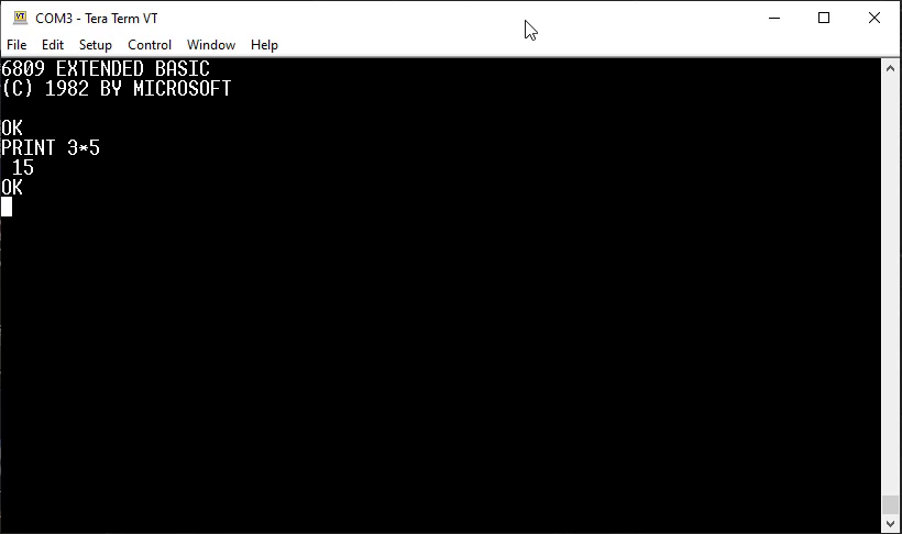
Perfect! We have Extended Basic booting up!
In addition, we still have up to 14 ROM banks, available for whatever else we might want to load up in the ROM Expansion Card (for a total of 16 banks available}.
It’s worth also noting that ASSIST09 itself takes just 2KB of ROM space, and actually provides a good foundation for writing your own ROM Applications.
ASSIST09 provides some useful system calls and also provides a start-up hook, for automatically running your extension code.

Also, I’ll just note again that I’ve run these tests with the CPU Card still being over-clocked at 4MHz CPU speed (using a 2MHz MC68B09 CPU).
Therefore, I’m pretty happy with how the Bus and new ROM Expansion Card are performing.
Now that I’m happy with the test results, I’ll add the ROM Expansion card PCB, and perhaps a couple of add-on pack options, to my Tindie Store. Just in-case anyone would like to play with one.
Other than that, my next intended ROM Expansion Card usage will likely be with a 6502 CPU Card. Perhaps with my original idea of re-creating the CreatiVision game console of the 1980’s.
But, more on that later…