
Recently, while working on my 6502 CPU Card design, I became aware of a small oversight on my existing 6809 CPU Card.
Nothing that has caused any issues, as I haven’t had any problems with using my existing v2.2 6809 CPU Card.
But it’s something I wanted to fix anyway.
Join me as I explain the oversight and walk-through the schematic and PCB changes made for v2.3.
There’s no real functional change with the update, therefore only a minor version number change from v2.2 to v2.3
What I’d noticed, is that I had used only a 2-pin header to allow the CPU’s R/W connection to the 28C256 EEPROM.
But, with the jumper not in place, the Write Enable (WE) pin is actually left floating.
When Write Enable is not used, it should really be pulled-high, to ensure that Write Enable remains in the inactive state.
But, as I said, this oversight has never caused me any problems in using the v2.2 Card.
So, to remedy this oversight, I’ve now implemented a 3-pin header, allowing a new Read Only jumper position, which implements a pull-up on the Write Enable pin.
While making this small change, I also took the opportunity to add a 2-pin Reset header.
This new header effectively just bridges the on-board Reset Button, to provide an easy header-lead connection, if you wanted to mount a reset switch elsewhere.
So with these two changes, I’ve updated the Schematic’s description and the PCB silkscreen to reflect v2.3.
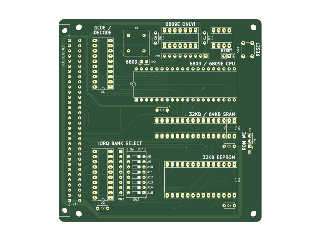
Here is the updated Schematic, showing the updated ROM jumper, and the new Reset header.
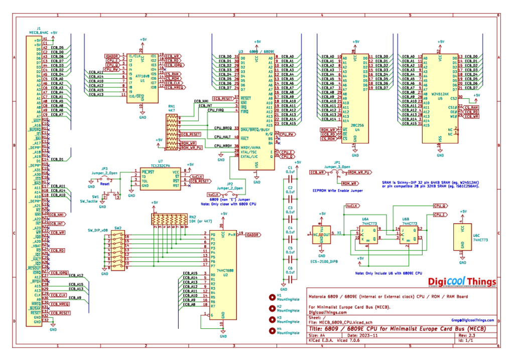
The BOM therefore just adds a 3-pin header, and we still have two 2-pin headers. One now re-purposed for the Reset header.
Here is the 3D PCB render, showing the updated ROM jumper, and the new Reset header.
I’ve now updated the MECB Github repository, and the Tindie store listing, to reflect the v2.3 changes.
This change was in place earlier this year, so if you’ve recently obtained a 6809 CPU Card PCB from my Tindie store, you’ll probably find you’ve already got v2.3
If you have the earlier v2.2 CPU Card, I’m sure these v2.3 changes will not make any difference to your Card usage.
As I’ve said, I have been using the v2.2 Card exclusively (without a jumper installed), ever since originally designing it, and I’ve never had any issues with any pre-programmed 28C256 ROM use.
However, if you are concerned, you can either install the jumper, so that ROM reads ensure that the Write Enable remains inactive (high).
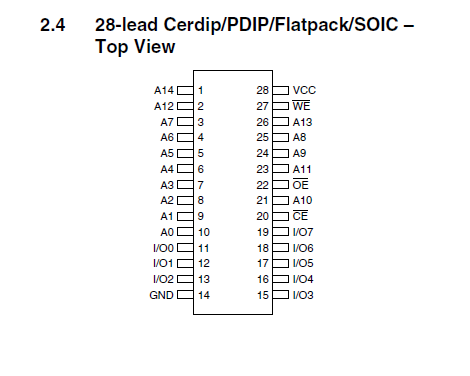
Or, you could install a pull-up resistor from the Write Enable pin (pin 27) to Vcc, which is the neighbouring pin 28. A 4.7K to 10K resister value would be appropriate.
Alternatively, you could also just simply solder-bridge pin 27 to pin 28, to directly connect Write Enable to Vcc.
However, if you take the solder bridge approach, I’d strongly recommend also removing the 2-pin header, as inadvertently inserting a jumper would then short the system R/W control signal to Vcc, which may damage your CPU.
Finally, while we are discussing the 28C256 Write Enable pin, it’s probably worth me also explaining why I included a jumper for this on the PCB anyway.
You see, the AT28C256 is an EEPROM (Electrically Erasable ROM). It is also conveniently accessed just like a Static RAM for both read and write cycles, so it’s easy to use for in-circuit writing.
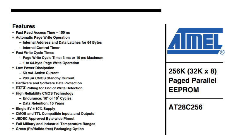
To write to the ROM you simply write a byte (or in fact up to 64 bytes consecutively, in the same page), and then you read the last byte written to poll for the completion of the write cycle.
Although a read occurs in a single 8-bit CPU cycle, typically with only 150ns access time, a write cycle can take up to 10ms.
Hence, the need to poll the last byte written with consecutive reads, until the correct data is read, signifying that the chip is once again ready for further read or write cycles.
So, the purpose of the jumper inclusion on the PCB is to allow experimentation with some code for writing to the EEPROM.
This can be useful for either making live changes to your ROM code, or perhaps for allocating an otherwise unused page of the ROM, to use for the non-volatile storage of system settings, or such like.
So, with that all explained, it’s time for me to get back to my 6502 CPU Card design.