
As I now have a modular retro 6809 computer system, with a flexible memory map, I thought it would be fun to mimic another simple 6809 system and to also get a BASIC Interpreter up and running.
Join me as I reconfigure our 6809 system’s memory map, and translate, adapt, and demonstrate an existing BASIC Interpreter for our MECB system.
First off, I’ll admit that I’m not really a fan of BASIC. I started out making systems based on 8-bit microprocessors, so I was used to having the power and speed of using low-level machine language on 8-bit microprocessors.
Therefore, I found Interpreted BASIC to be too slow and restrictive. But, the worst was seeing a teacher, teaching kids how to write unstructured spaghetti BASIC code, littered with GOTO statements, that was totally unreadable (I was one of those kids!).
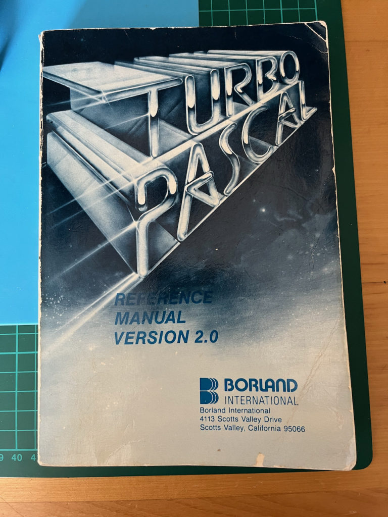
Eventually, my initial high-level language of choice was the wildly successful Borland Turbo Pascal compiler which I enjoyed coding business solutions on early IBM PC clones.
However, getting back on topic, as BASIC is the de facto standard amongst retro 8-bit computers, I thought it would be a fun exercise to see how quickly we can get a BASIC Interpreter up and running on our MECB 6809 system.
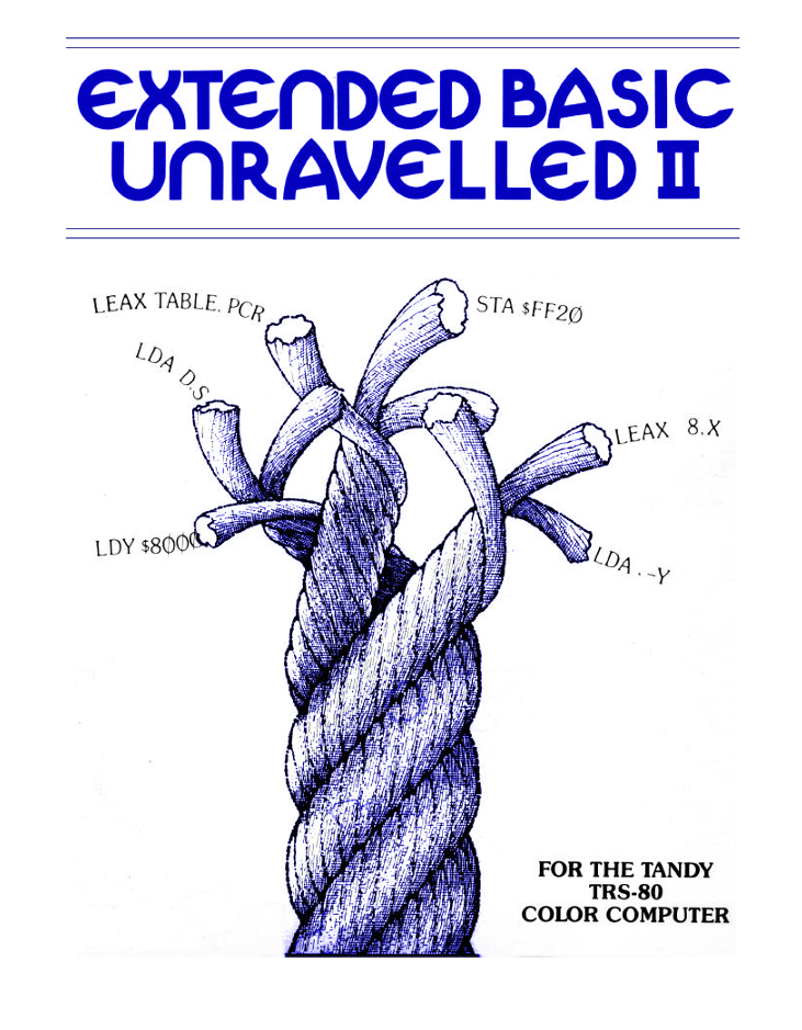
From a quick google search, I landed on Grant Searle’s minimal 6809 Computer design, where he utilised the TRS-80 Color Computer Extended BASIC, as his choice of a good 6809 BASIC.
Now there were a couple of things I needed to take care of.
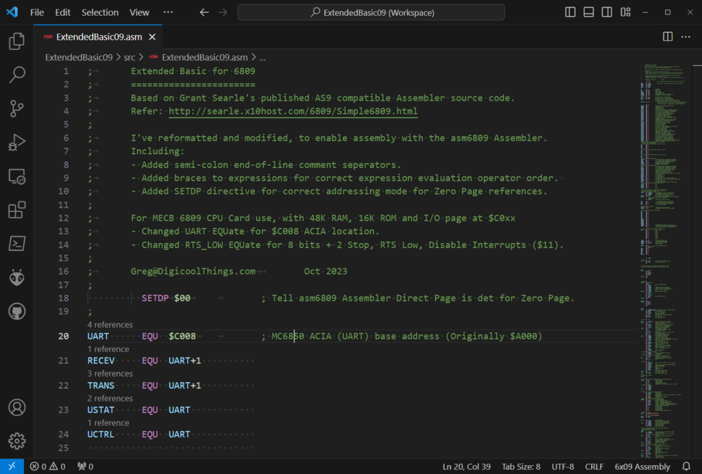
Firstly, Grant’s 6809 design is based on a memory map with 32K of RAM, 16K of ROM space, and a MC68B50 ACIA located at address $A000.
Our current 64K memory map configuration on our MECB 6809 system has 56K of RAM, and just 8K allocated for ROM space, with the ACIA located at $E008.
Since the assembled BASIC ROM comes in at just under 10K, our existing 8K ROM space is clearly inadequate.
Thinking ahead, we should probably allow for the possibility of adding some TMS9929A Video Card support, or some Sound support to the BASIC. Who knows?
So, I was therefore thinking that the 16K of ROM space allocation probably sounds about right.
I’d then naturally allocate the remaining 48K to RAM, and move the I/O page to still be at the beginning of the ROM space (or $C000).
If I left the Motorola I/O Card’s existing memory decoding as it currently is, that would then put the MC6840 PTM at $C000, the MC6850 ACIA at $C008, and the MC6821 PIA at $C010.
Sounds good to me.
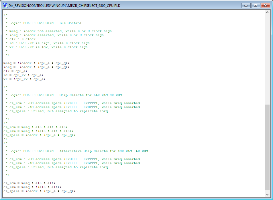
So this just involves a change to the 6809 CPU card’s PLD, to re-assign the ROM and RAM chip select address space allocation.
Also, a change to the CPU card’s I/O Bank select DIP switch, to put the I/O Bank at $C0xx, instead of $E0xx. Or, specifically, we just need to toggle the Address line A13 switch to low, so we’ve just got A15 & A14 set high (to select the $C0 bank).
Let’s take a look at WinCUPL for the PLD change.
Next up, is the second issue.
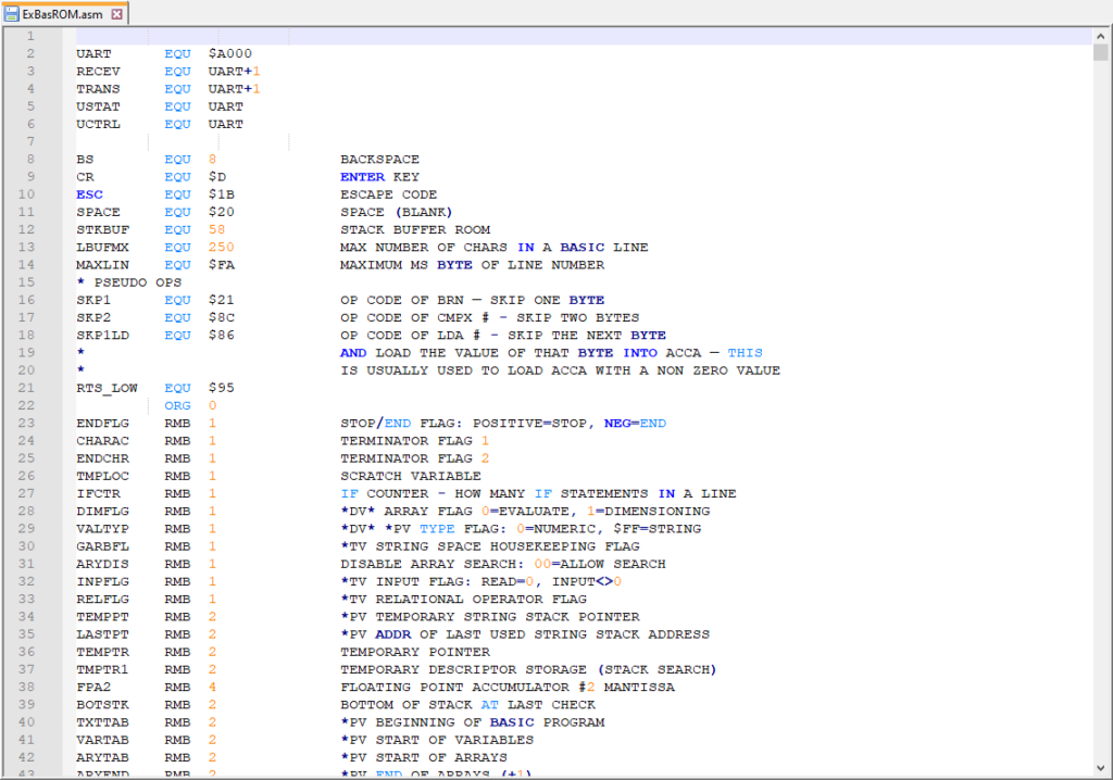
Grant’s version of the BASIC source is formatted for the old school official Motorola AS9 cross-assembler. This original assembler has some quirks.
Firstly, I think AS9 requires a DOS system to run.
Secondly, one of the old Motorola Assembler standards is simply prone to allowing errors in your code.
This is where the Motorola syntax allows a comment to follow any operands, separated only by blank space.
This means that if you inadvertently mis-type an operand, the start of your comment might be taken as part of the operand, without generating errors, and creating unintended code!
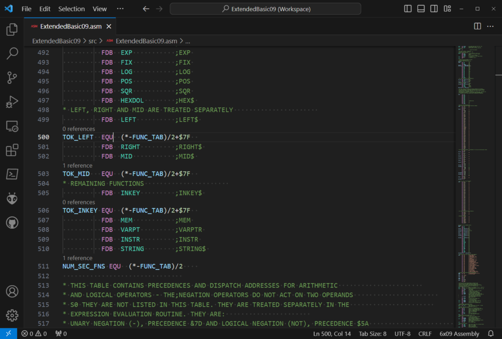
Another quirk of AS9, that I discovered, is that the expression evaluation doesn’t follow the normally expected operator precedence. Instead, it just evaluates expressions strictly left to right.
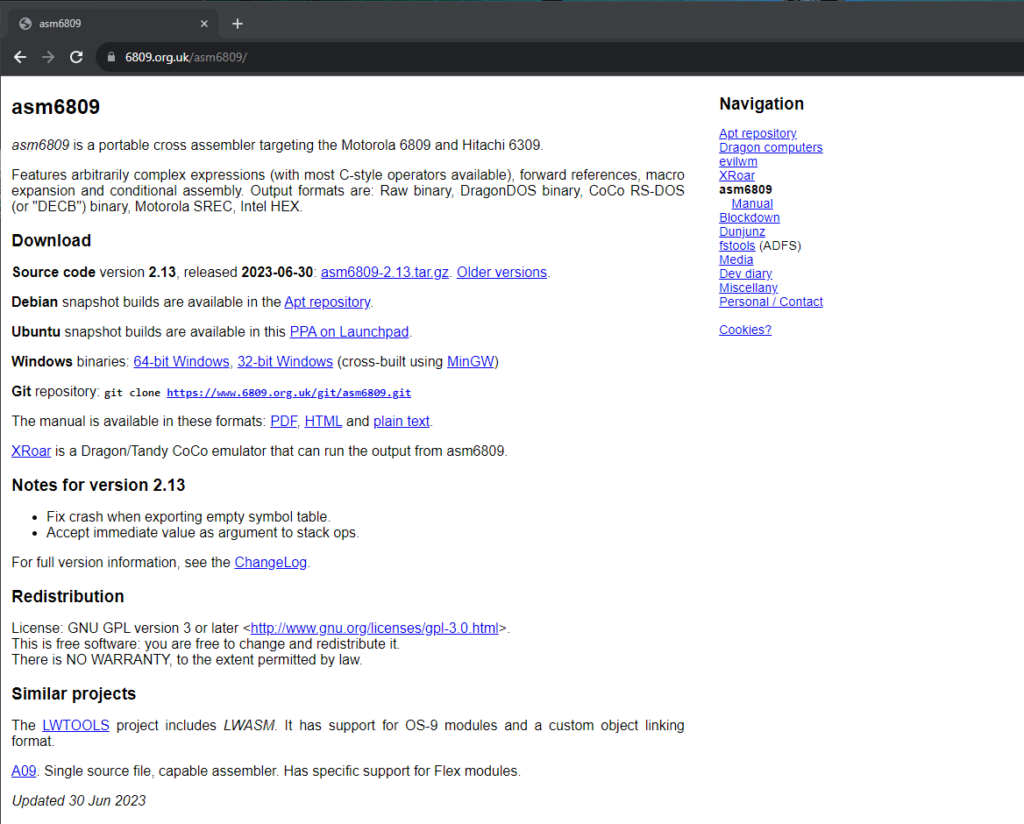
So, I decided that the first thing I should do is reformat the source code to allow assembly with the asm6809 assembler, which I have been using. asm6809 is a more refined cross-assembler, and also supports the Hitachi 6309 extensions.
So first I needed to fix the missing semi-colons, to properly identify end-of-line comments.
Fortunately, I noted most of the comments started from column 31 of the source.
Therefore, I decided to use Visual Studio Code’s regex based search & replace, to swap the 30th character in each line from a space to a semi-colon, where the 30th character was a space, and the space was followed by one or more non-space characters.
Here’s the regex I used in the search option.
(^.{29}) ([^ ]+)
Description:
- ^ – Anchors the match to the beginning of the line.
- .{29} – Matches any 29 characters (including spaces).
- space – Matches a single space character at the 30th position.
- [^ ]+ – Matches one or more non-space characters after the space.
The two groups of braces () capture the before space, and the after space characters.
Then, to replace the above located space character with a semicolon (;), I specified the replace as:
$1;$2
Description:
- $1 – Is substituted with the first capture (i.e. characters before the space).
- ; – Inserts the semicolon character ; (i.e. in place of the original space).
- $2 – Is substituted with the second capture (i.e. characters after the space).
This search & replace resolved 99% of the commenting issue, leaving only a few lines to fix, where the comment didn’t start at column 31.
With the comment issue resolved the next issue was ensuring that the asm6809 assembler used the correct addressing mode for the zero page.
To resolve this, I noted that the 6809’s DP register is untouched by the code, therefore on reset the DP register just defaults to the zero page and remains unchanged.
We therefore just need to tell the asm6809 Assembler about this, with the SETDP directive, so the assembler will use the most efficient addressing mode when accessing page zero.
Next we needed to deal with the operator precedence issue.
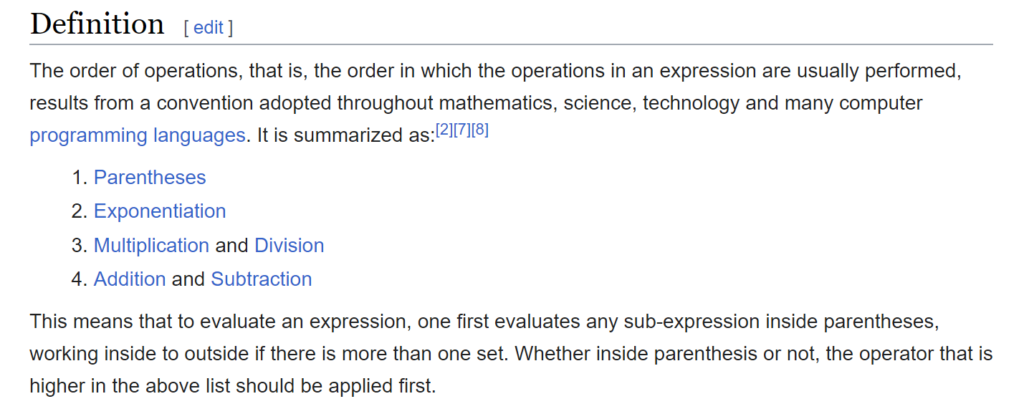
There are a number of code lines where an expression involves subtraction and division, with the subtraction appearing before the division.
To have these expressions evaluated correctly with asm6809, which follows correct operator precedence, we need to add some parentheses around the leading subtraction, to ensure that it’s processed before the division is, so we get the intended answer.
Having made all these changes, and with successful assembly, the final step was checking the assembled binary file result.
Grant had published an Intel Hex assembly of his AS9 version of the Basic.
I was therefore able to assemble an Intel Hex version with asm6809, and confirm that the byte output of the assembly was identical.
Interestingly, this exercise actually highlighted an apparent typo with Grant’s original source.
A CMPA instruction operand at line 5075, specified Direct addressing mode, with a $ character, instead of Immediate mode, with a # character. Other than this correction to my asm6809 translation, our assembled hex files were identical.
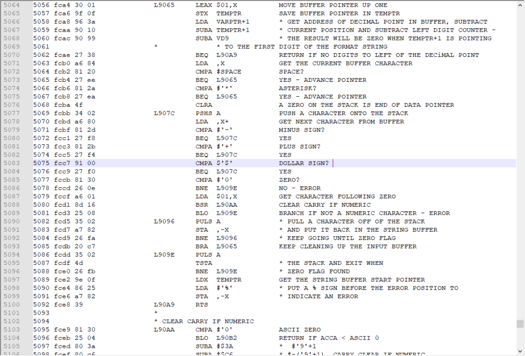
I’ve sent an email to Grant to alert him of this apparent error in his published BASIC code.
So, finally, now that I have a safer version of the assembly source, that I can assemble with asm6809, I think I probably just need to make two initial changes to the code to allow it to run on for our MECB system.
Firstly, changing the ACIA address from $A000 to $C008.
Secondly, I need to disable the ACIA interrupt, as Grant was using the IRQ output of the ACIA directly, to implement a RTS function.
Our ACIA IRQ output is connected to the CPU’s interrupt, as you’d normally expect.
So if we wanted an interrupt driven serial interface, we’d need to investigate an interrupt service routine to handle that.
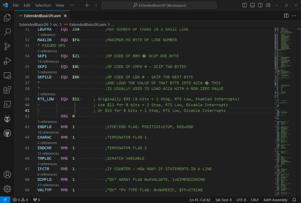
To resolve this we just need to redefine the ACIA Control Register initialisation byte, which is stored in the RTS_LOW EQUate.
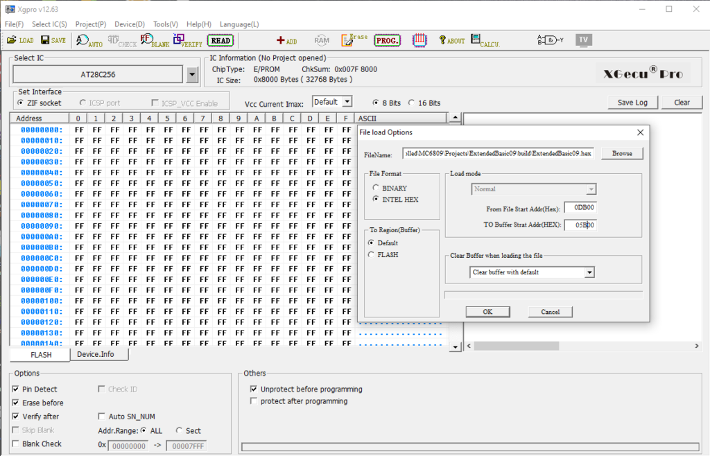
So, with these changes made and a new Intel Hex file generated with the asm6809 assembler, we just need to program our 28C256 ROM chip.
As we have a 32K ROM (28C256), we also need to tell our programmer to load the assembled code, which starts at $DB00, into the ROM space starting at $5B00, effectively offsetting the code so that it appears at the top of our 32K ROM chip.
With the ROM and our PLD chips programmed we then got the replacement chips installed on our CPU card.
Finally, I switched off the I/O Select DIP switch’s A13 address line, to change over to the $C0xx I/O page.
With this done, we were all ready to go, with our system now configured for 48K of RAM and 16K or ROM and our I/O devices now in the $C0xx memory page.
So, next we truned it on to see what we get…
And we were looking good with our Microsoft Extended BASIC startup.
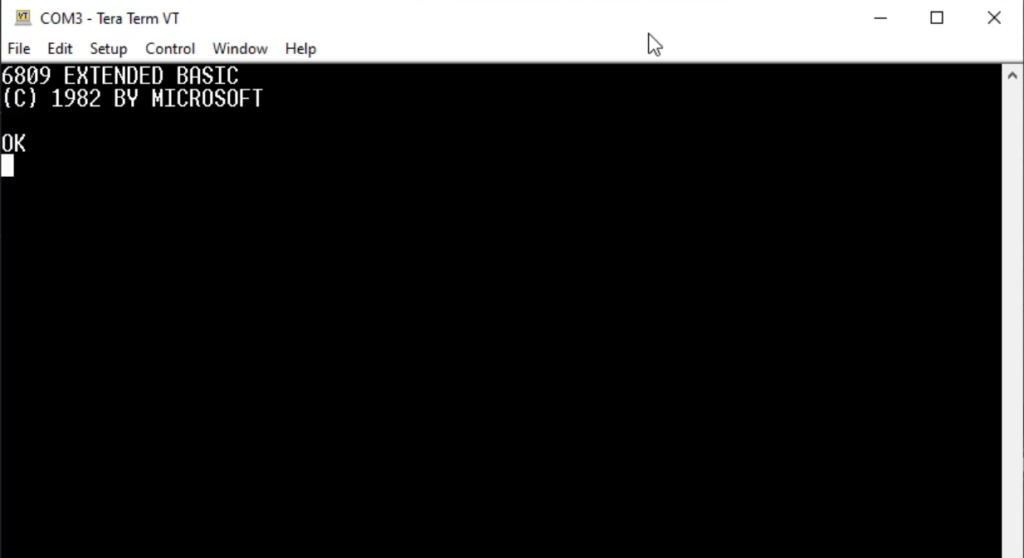
Now we were up and running, we first check the available memory, by executing PRINT MEM
And we got: -17136
Interestingly this appears to show that this version of BASIC was written for a system that could have a maximum of 32K RAM.
The decimal value of -17136 is the 16 bit 2’s compliment equivalent of hex $DB10, so this does equate to our 48K of RAM.
A 2’s compliment 16 bit number can of course only represent a positive decimal integer value of up to 32767.
So, our 48K of RAM is being recognised, just not able to be reported appropriately as just under 48K available.
Note that the existing BASIC code dynamically determines the available memory by stepping through the memory space with a RAM test, to locate the end of RAM.
What I found interesting, is that the test extends beyond 32K, even though the 2’s compliment reporting of the MEM value is limited to 32767 bytes!
So, lastly I finished off with a simple “Hello World” loop, just to check that our BASIC Interpreter appears to be working as is expected.
10 PRINT “Hello World! “;20 GOTO 10
To check our program listing in memory, I typed:
LIST
And finally, to run the code:
RUN
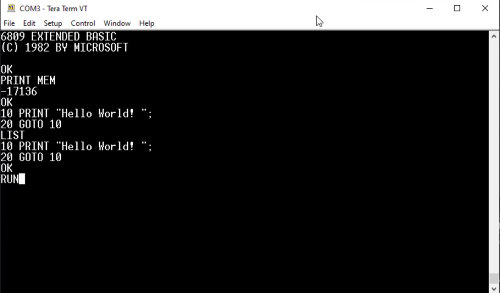
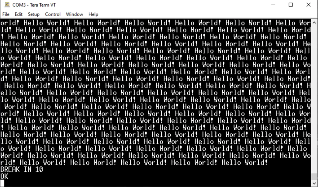
Okay, we appear to have successfully got Extended BASIC up and running on our MECB 6809 system!
I’ll be sure to put the asm6809 compatible assembly source, the assembled Intel Hex file, and a 32K ROM binary image file up on the MECB GitHub repository, for anyone interested in playing with this.
Have fun!
Excellent!
A question though – and perhaps I need to watch this again, but did you move the logic for buffers to a different location, and wouldn’t that also mean any plc’s on other cards need to correlate with this? I’m imagining it might make sense to standardise on a particular architecture, but the flexibility of the system as it sits, would probably enable tinkerers like myself to emulate certain other architectures down the track based on the cpu card plugged in? Even if we didn’t have cartridge interfaces for these systems…
Anyhow, a very nice article – informative & helpful!
😀
Apologies, but can you please elaborate a bit more on your question. I’m not sure what you were referring to by “logic for buffers”?
Alas, no, it seems I just needed to rewatch it! – I saw the PLC reprogram to accommodate the 16k rom and later the change in the assembly code for the address range used for the I/O and somehow made an unholy abomination in my head with it all. But now I’ve sorted that out, understanding the use of 16k rom and the modding of the assembly to accommodate the I/O range this system uses, I can go back to pondering my first world issues – like, I imagine it wouldn’t be too difficult to have a cartridge style system to usurp the in-built rom, if for example there were some kind of instant on gaming or productivity I had in mind, a-la C64 or Tandy CoCo? That would be different to the addition of a mass storage device, such as an SD card or Compact Flash, right?
Interesting that you should mention thinking about a cartridge style system. I was already planning on making a ROM “Cartridge” card. You see, once I finish my 6502 CPU Card I was thinking of emulating a Creativison (Dick Smith Wizzard) console system, with the 6502 CPU Card, Motorola I/O Card, and TMS9929A VDP Card. This then leaves the fourth Backplane slot free (as well as the horizontal slot), allowing for a ROM “Cartridge” slot. Via the CPU Card’s PLD you could either fully disable the CPU Card’s ROM, or perhaps limit it to just a smaller BIOS. Then the ROM Card could be configured for it’s own address space. I was also thinking that if I used something like a bigger 27C040 EPROM (which is 512KB), then a memory bank switch could allow any one of 16 Banks of 32KB (for example) to be selected, for different game cartridge images. I’m still focused on the 6502 CPU Card at the moment, but these are the possible future ROM “Cartridge” Card thoughts I’d also been pondering.
Oh, Excellent!! 😀 I look forward to that! I originally imagined that dipswitch selector on the CPU card to select an appropriate bank and size of rom to use at runtime, but a secondary case was that cartridge I could use instead to override the basic temporarily in the system to run, say, Assist09 or some kind of DOS or Unix, etc. I originally imagined an MECB card that had multiple cartridge slots, similar to the MSX architecture that allowed for memory expansions or specialised I/O on top of utility/games/productivity cartridges, and I’m already imagining a minor redesign to the case I have designed for this to accommodate, but I’ll await some non-virtual examples of this MECB system to be in my hot little mitts before I run it past you…
To retain modularity and flexibility, I think it is important that each card is self contained. i.e. The PLD on the CPU Card just defines the address space allocation of the memory on the CPU Card itself. If an additional memory card is present, then you’d configure the CPU Card memory allocation to not conflict with other cards you intended to insert. So, you might only allocate a portion of the CPU Card’s memory (e.g. some RAM space), and turn the ROM off. On the ROM (cartridge?) Card, I’d envision a similar Card specific PLD that would allocate a non-conflicting range of the 64K address space. So, you could (for example), disable all ROM on the CPU card, and map the ROM Card’s PLD to utilise the top 16KB of the 64K CPU address space. Then, have a seperate bank select switch on the ROM Card to maybe select one of 16 banks of the total available ROM to occupy this 16KB space. In this way you could have switch control of whether you booted the CPU Card with ASSIST09 ROM or BASIC ROM etc. (in the 6809 case). I imagine having a header on the PCB as well, so you could have a case mounted switch for ROM bank selection. Just thinking out loud.
You know something else I thought of – and I guess it would depend on pin availability on the bus, but if there were a few available pins, it might be possible for the cpu card to signal itself to the bus in a way that, for example, a rom cartridge would select an appropriate bank containing the instruction code specific to that cpu? Maybe three pins in a bit count that could be passed through via the plc on the cartridge to do such selecting? Same for other architecture specific hardware to either work appropriately with the architecture in use, or at the very least, indicate in a sane way that it’s not going to play with the current architecture discovered on the bus? I’m thinking of a C64 emulation/sound IC/cartridge socket card that would expect to find a 6502, or disable itself and isolate hardware from the bus if some other cpu card were operating, etc.
I know this is still distant plans, but if forward architecture planning were a thing, something to consider… no idea how far along you are with it all, of course.
😀
The standard ECB 64 pin 2 row A&C BUS has pins allocated for upto 24 pin Address Bus (A0 – A23). You can see these pins identified on my schematics. So, instead of a manual bank select switch, it would be feasible to have a CPU Card with a MMU (memory management unit) to allow extending the address bus to 16MB (24 bit), or even just 1MB (20 bit). The MMU could be as simple as an output register that the CPU could write to. You could then, in theory, have the CPU control switching ROM banks on a seperate ROM Card. The ROM card banks would therefore be controlled by the A16 – A23 BUS Address pins, instead of via a manual bank select switch. This would require a BIOS on the CPU card to boot into and control the bank switching. The simplist would be to just boot ASSIST09 on the CPU Card (in just 2KB of ROM), and then map say 14KB (or 30KB) as a switchable ROM bank, with maybe the low 32KB for RAM. Then you could switch banks from ASSIST09 (or any RAM resident software), by writing to the bank register and then calling the code in the selected ROM bank. There are of course more complcated MMU systems we could devise, but then it’s starting to get away from the original intent of MECB (as in “Minimalist” etc.). 😉
Ooh, another thought I had following on from the previous post (no edit feature… -_- Sorry!), but this “architecture feature would also proof the system itself from multiple cpu cards being plugged into the bus at the same time – to save people like me from myself – each cpu card would look for more cpu identifiers than it has to ensure it’s not competing, and if it did find another cpu architecture connected to the bus, it would as I mention, isolate itself from the bus – other features this would enable, for example, hardware specific idioms required for each cpu, you mentioned the Z80 has a fixed I/O range, but it might be that an I/O card with joystick ports might have to act differently or use a different port depending on the cpu, or perhaps a single display or I/O card that works with all cpu architectures by swapping in/out on-board ICs and logic to accommodate rather than having to match a series of cards for a particular cpu architecture (which I imagine would make for a cluttered I/O card with multiple architecture specific ICs on-board), then of course, a display card that would use system ram/video ram/ or whatever that abomination the Atari 2600 used before either of those existed – and for hacking purposes, perhaps a multi-cpu architecture could also be tolerated by the addition of more bus pin identifiers/indicators, but I’m sure multiple cpu systems are not a trivial exercise you’d be planning for with these hobby systems – my imagination is telling me there’s plenty to do with this already! 😀
Maybe it’s time to publish a roadmap and feature request somewhere…?
…or maybe you shouldn’t with people like me hanging around here!
xD
Yes, I’m not currently planning to support multiple processor arbitration, this is more complex than the intent of MECB. Regarding a roadmap, the closest I’ve come to a published roadmap is my noting of Cards that I have in progress or at the planning stage, which is on my MECB homepage. Perhaps eventually something like a Forum would help public discussion of different ideas. But, until others start developing their own MECB Cards, I’m pretty much just progressing with my own vision of what I want to play with next. Our discussion has helped though, as I now have a more considered view of a design for my initial ROM Expansion Card. This has also allowed me to ge ta bit of a head start on ordering some parts, while I continue work on my 6502 CPU Card.
Something else I had in mind – if I had a handful of recovered 64k rom chips, wouldn’t it be possible to setup a multi-cart like system for multiple rom images on the one rom chip, selectable in size from 4k to 16k, and selectable sections in 4k block resolution with an on-board set of toggles as currently used to determine the Bank Select? Maybe some more fancy plc footwork to be had, and probably a cpu card redesign to accommodate another bank of switches, right?