
Earlier, I posted an article and video on my TMS9929A Video Display Processor (VDP) rediscovery. This included designing an alternative Retro VRAM solution, which I then implemented as a breadboard prototype and also verified successful operation.
Having built an MECB backplane, and my first actual MECB card (a Prototype card), and also having proved the PLD based address decoding logic, now seems like a good time to implement my TMS9929A based VDP circuit design onto a PCB, as my first MECB Video Card.
I’ll also be able to use the header pins on the MECB Prototype card to allow me to easily hook-up the same Arduino test setup, which I’d used with the breadboard circuit. This will allow an initial test of the PCB design with a known working test setup.
Ultimately, we’ll (of course) add our first MECB CPU Card to the project, then we’ll be well on our way to our first full MECB based Retro 8-bit computer design.
But, before I get ahead of myself, I’ll focus on the creation of my first MECB video card. That is, a TMS9929A (or TMS9928A) VDP based, alternative Retro VRAM solution, Video card.
To start with, on my workbench I have the breadboard setup that I built and proved operational in my earlier TMS9929A rediscovery video. You can find this described in detail in my post TMS9929A VDP Rediscovery and Alternative Retro VRAM Solution. I’d suggest reading that post / watching that video first, where I discuss the design in detail.
So, let’s dive into the KiCAD schematic. As you can see, the TMS9929A and 4464 based VRAM solution is basically just as I’d earlier prototyped. All that I’ve essentially added, is the MECB bus connector, as well as a PLD for address decoding. Also, for the output, I’ve added a mini-DIN RGB connector, as well as a stereo audio input to allow sound pass-through to the mini-DIN RGB connector.

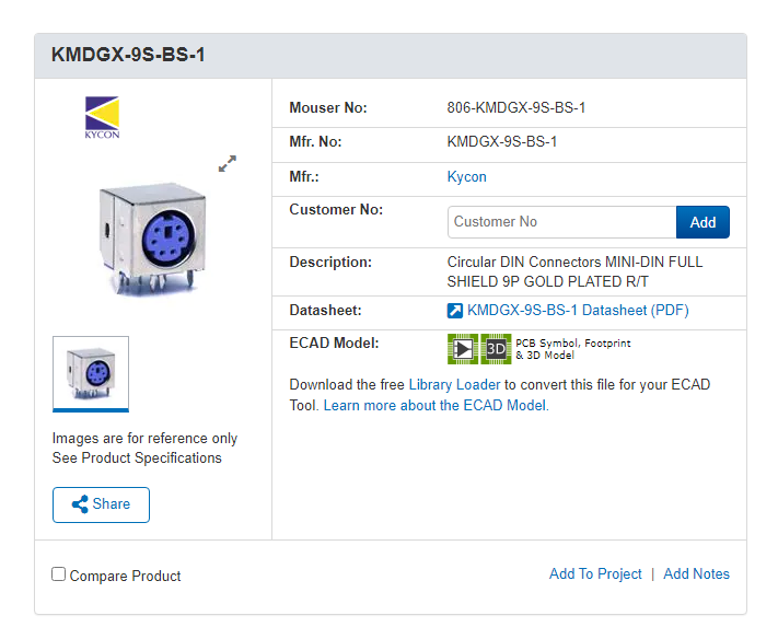
The choice of which RGB connector to use, pretty much boiled down to choosing between the use of an 8-pin mini-DIN, for the more recent XRGB retro RGB connection cable standard. Or instead, using a 9-pin min-DIN, as used by the Sega Genesis 2 (or Mega Dive 2).
This decision proved reasonably easy. I quickly found that 9-pin mini-DIN PCB mount connectors and retro Sega Genesis 2 RGB cables are very easy to find and are relatively inexpensive. Whereas 8-pin mini-DIN PCB mount connectors and pre-made XRGB cables were harder to find and considerably more expensive!
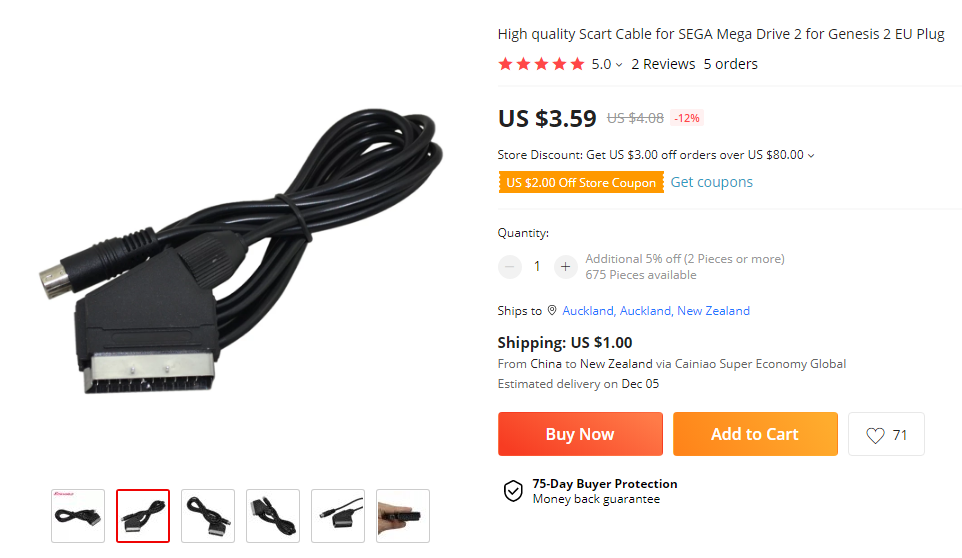
The only downside with choosing the Genesis 2 standard is that the commonly found Genesis 2 RGB SCART cables include 75-ohm output resistors (and capacitors?) within the actual cable assembly.
This meant either modifying the TMS-RGB board’s 75-ohm SMD output resistors with bypass links (or swapping out for zero-ohm SMD resistors), or, modifying the Genesis 2 cables to remove the resistors.

I’ve chosen to remove the resistors from the cheap pre-made Genesis 2 SCART RGB cables, as this is reasonably easy to do and this approach retains the resistors on the TMS-RGB board, which is, quite frankly, where the 75-ohm output resistors belong!
So, let’s take a look at the PCB layout. As discussed in previous MECB related posts and videos, I created this KiCAD project by using the standard MECB board KiCAD template which I originally created. This sped up the VDP card design process significantly, by letting me start-off with a pre-defined PCB with the mounting holes, the bus connector, and the address decode PLD already in-place and the PLD’s traces already routed.
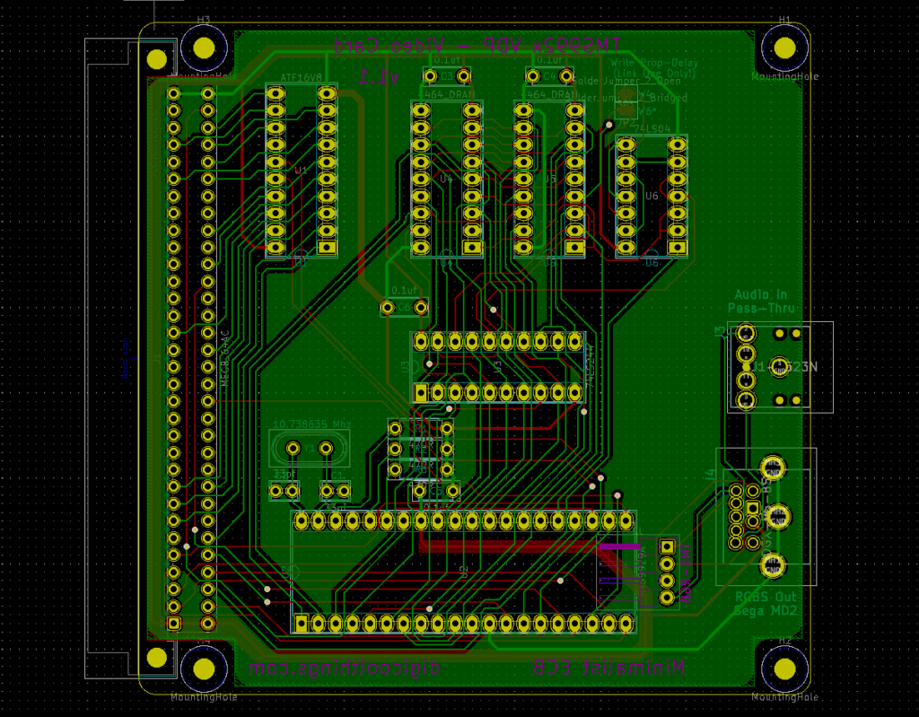
As you can see, the rest of the PCB layout came together relatively nicely, with plenty of space available on the MECB standard approximately 100mm square PCB size, to allow for relative ease of trace routing with a simple and cheap 2-layer board.
I then order the initial v1.0 prototype PCBs from JLCPCB. Once they arrived, it was time to put the first one together.
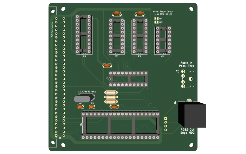
I started off with soldering in the resistors, and then the regular IC sockets. Then I fitted the capacitors and the crystal. After which, the DIN 41612 MECB bus connector and the Zero Insertion Force (ZIF) IC socket which I decided to use on this build, for the easy swap-outs of the address decode PLD chip. Finally, I soldered in place the Video and Audio connectors.
In terms of the overall assembly, the only part I didn’t mount, as yet, is the TMS-RGB module. This mounts on the back of the PCB, but I’m intentionally not permanently mounting it as yet, as this prototype PCB is (at this point), untested.
Normally the TMS-RGB module will just drop in place on the back of the 40-pin VDP IC socket and is then soldered permanently in place via the relevant connecting pins. Also, I implemented a 4-pin right angle pin header on the PCB, to connect the TMS-RGB module’s outputs back to the PCB, where the RGBS output signals are then routed to the mini-DIN output connector.
So, for the purposes of initial PCB testing, I just temporarily wired a TMS-RGB module onto the appropriate connection pins, swapping across the module that I’d been using from the breadboard circuit. This enables me to initially test the PCB design is actually working, as designed, before more permanently mounting the module.
Once the TMS-RGB module was wired up, I went ahead with getting the regular ICs inserted. First was the 74HCT04 hex inverter. Then the 74HCT244 octal buffer. Then a couple of 4464 Dynamic RAMs. Finally, the TMS9929A VDP itself.
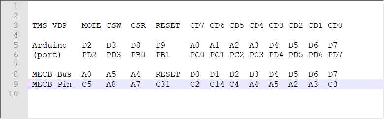
To setup for testing the new MECB Video Card, I used the MECB Prototype card, connected to the MECB backplane’s horizontal connector, to provide easy access to the MECB bus header, to facilitate connecting up the Arduino test setup.
As the Arduino was programmed to connect directly to the TMS VDP chip, and the Chip Select pins are now routed on the PCB via the address decode PLD, I decided to program a PLD so that a couple of the address lines are simply passed directly through to the VDP’s Chip Select Read (CSR) and Chip Select Write (CSW) pins.

This enables me to initially test the full VDP PCB without making any changes to my existing Arduino code. So, the PCB test should replicate how it was previously working on the breadboard, only now with the full 8-bit wide video memory in place. Remembering, that for the proof of design breadboard prototype, I had just connected up a single 4464 DRAM chip, which provided just the low nibble of each video memory byte.
So, the next step was programming the PLD with the simple pass-through configuration. This effectively just connects the Bus Address line A4 to the VDP Chip Select Read (CSR), and A5 to Chip Select Write (CSW). It’s also noted that the VDP’s “mode” selection input pin is already wired directly to Bus Address line A0, so only the CSR and CSW inputs require the PLD pass-through.
After inserting the programmed PLD into its ZIF socket, I then swapped the Arduino across from the breadboard circuit. To do this, I got some Male to Female Dupont leads, so that I could jumper from the Arduino’s Female headers to the MECB prototype boards Bus connection Male headers.
By referring to the Arduino Sketch notes, I then mapped these required connections to the appropriate MECB Bus pins, so I end up with the following required connection map. Note, the only connection I’ve omitted from this connection map is, of course, the common GND connection between the MECB power and the Arduino. So, I got that connected first, before I forgot!
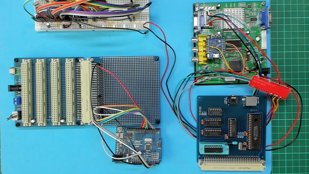
Finally, to complete the wiring for this test, I connected my GBS-Control VGA convertor power input to the spare MECB backplane screw terminal power connector. This proved very convenient. Although, as the screw terminal is one of the optional MECB backplane’s power inputs (so is not switched via the power switch), it will be fine that the GBS-Control VGA convertor is permanently powered.
Now, ready to test, I connected up my VGA monitor to the GBS-Control VGA output and connected my USB-C power adapter to the MECB power input and switched on. No magic smoke! So, all that remains is to power up the Arduino board!
So, lastly, I connected up the Arduino to my PC USB port, and we were up and running!

Needless to say, I was a little blown-away that this ALL worked first time! Although I was confident in the PCB design, the chances of an error somewhere in the wiring up of everything was always on the cards.
But, not only did the PCB work on first power-on test, the video output was rock solid and completely video artifact free! There had previously been a little video noise evident on the earlier breadboard prototype, which I had just associated with the breadboard circuit. So, it was great to see that once the design was implemented on a proper PCB design, this was indeed resolved.
Also, the signal path will be even cleaner once the TMS-RGB module is permanently mounted and the mini-DIN RGB lead is in use, to get rid of the last jumper wires.
With the MECB VDP Video Card now finally successfully tested, my next step will be to play around a little with the Arduino code, to utilise the full 8-bit wide video memory (and ensure all 8-bits are now being memory tested), after which I can switch my attention to my first MECB Bus CPU card!
Follow-up
As a follow-up to my original video (linked at the top of this article), I created a follow-up video (linked below).
The original video ended with the successful initial test of the first PCB build for my TMS9929A Video card. However, it also ended without the final completion of the PCB, the modifications to the Genesis 2 RGB cable, or any testing using the full byte wide video memory, that we now have on the final PCB!
So, please join me once again for a quick follow-up video, where I show the finalised PCB, output video cable modifications, and then also update the Arduino test code to take full advantage of the now byte wide VRAM of the finalised card.