
TL;DR
The TMS9929A / TMS9928A / TMMS9918A are Video Display Processors produced by Texas Instruments in the Retro 8-bit era of the early 1980’s.
They were used in a number of 80’s systems, including the ColecoVision, CreatiVision, SpectraVideo, MSX, and Texas Instruments own TI-99/4A Home Computer.
Join me as I rediscover my own TMS9929A experience from the 80’s, and recreate a TMS9929A circuit utilising the latest optimal video output, and go about designing an improved alternative Video RAM solution.
I walk-through my design process, before demonstrating the working solution, with a walk-through of my Arduino sketch which fully tests the improved VRAM solution with multiple pass, multiple bit-pattern tests.
My alternative VRAM solution comprises just 4 ICs (totaling just 70 pins), significantly less than the original 128 pins (8 ICs), or the 102 pins (5 ICs) of a 2010 published Static RAM solution.
Background
Recently, I missed out on an opportunity to buy an old Dick Smith Wizzard computer / gaming console. Randomly discovering this auction listing brought back memories of working for Dick Smith in the 1980’s, when we imported the Wizzard as one of the earliest colour computers available to New Zealanders.
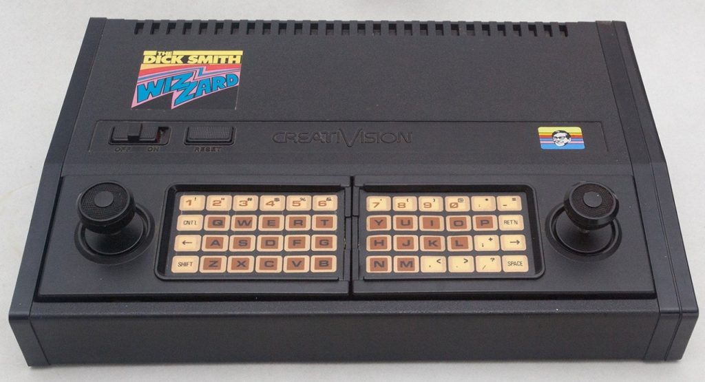
The Wizzard was of course just the local Australasian branding of VTech’s CreatiVision system.
This got me researching the CreatiVision, to reminisce about the exciting games we were able to play in colour when these consoles first arrived in New Zealand. A country that had strict import restrictions in the early 1980’s, meaning that most New Zealanders had not seen a colour gaming console, capable of playing arcade style Space Invaders and Pac Man style games, that you could actually play on your own television. It was an exciting time!
I never owned a Wizzard back then, as it was priced well beyond my lowly paid teenage pay packet, and all of my money had gone into a System 80 in those early personal computing years.
TMS9929A Video Display Processor (VDP)
Re-discovering the Wizzard / CreatiVision reminded me that it was based on the 6502 CPU and the TMS9929A VDP.
I’d spent plenty of time on 6502 assembly code later in the 80’s (mostly on the Commodore 64), and I also had a TMS9929A somewhere. I recall I’d wired one up on a Wire-Wrap board to experiment with, just like various other early video display processors I’d experimented with, back in the day.
Locating the CreatiVemu pages and forum (at www.madrigaldesign.it), provided some good schematics and other technical information on the CreatiVision.
So this was enough to trigger me into digging out my old TMS9929A chip, to once again have a play with it. I even found my original photocopied preliminary datasheets for this VDP, in my boxes of old design notes and datasheets.
Note that the TMS9929A provides PAL Video timing, there is also the TMS9928A (and TMS9918A) that provide NTSC timing.
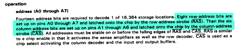
Firstly, some research, to discover what others had done with this chip in more recent times. As many will know the TMS9929/28/18 originally utilised triple-power supply 4116 Dynamic RAM chips, and also typically used a colour encoder chip to produce a composite video signal (usually to an RF modulator output). Due to this, the video output quality seen on old RF input televisions of the time, was never fully up to what the TMS chip was actually capable of producing.
Obtaining Optimal Video Quality via TMS-RGB
Some hunting around determined that after several evolutionary projects, each one building on the findings of others, the TMS9929/28 optimal video quality output has recently been nicely resolved with the TMS-RGB add-on module.
This 40-pin DIP sized module sits nicely on a PCB’s underside, attached underneath the TMS chips 40-pin DIP package or (preferably), IC socket. This means the TMS-RGB module can pretty much be retro-fitted to any TMS9929/28 based system.
So, getting great video output from a TMS9929/28 VDP is a nicely solved problem!
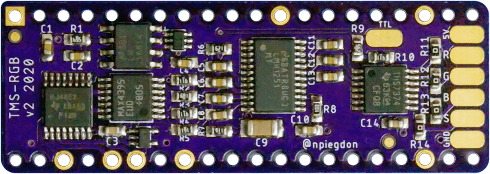
The TMS-RGB module was created by Nicholas Piegdon. You can read his TMS-RGB Development Story here.
An Alternative Retro VRAM Solution
Which RAM chip(s) to use?
Firstly, I’ll point out that there is a later, but less common, TMS9129 / TMS9128 / TMS9118 VDP variant which instead uses 2x 4416 Dynamic RAM chips. However, TMS9129 chips are much harder to obtain and significantly more expensive.
So, the next piece of research was to investigate an alternative to the 8x 4116 Dynamic RAM chips, used for the 16K Bytes of TMS9929A Video RAM. Clearly, we should be able to avoid the need for a triple power supply, as just a single 5V power supply is desired.
This lead me to a PDF document dated January 2010, titled: “SRAM Replacement for TMS99x8 VRAM”, by Tom LeMense. This appears to be the VRAM replacement approach still being used by even the most recent TMS99xx VDP based projects, that I could find. You can read Tom’s TMS9918 VDP with SRAM video memory story here.
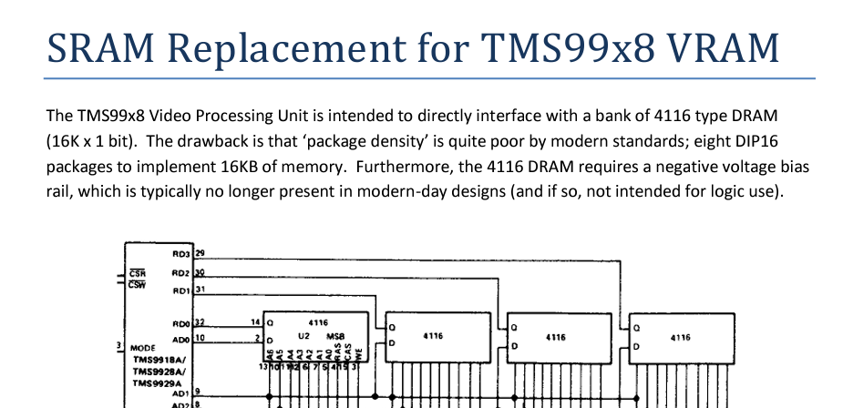
Although this SRAM solution is over 10 years old, and appears to be a proven approach, I wasn’t overly happy with replacing eight 16-pin chips, with a five chip solution that included a large 28-pin chip, three 20-pin chips, plus a 14-pin chip.
You are, therefore, replacing an original 128 pin count memory chip solution (8x 16-pin), with a 102 chip pin count. Sure, you are achieving a single 5V supply solution, but in terms of the PCB real estate and PCB routing, you’re only saving just 26 pins.
So, I thought I’d try a different approach. I didn’t see the need to implement a Static RAM solution, as retro Dynamic RAM chips are relatively cheap and easy enough to get your hands on. In addition, the later DRAM chips were more reliable than the earlier 4116 devices. Also, sticking with DRAM would avoid the need to demux the Address output.
The first seemingly obvious approach, was to look at replacing the eight 4116 16Kx1 chips with a couple of 4416 16Kx4 chips, as used by the rarer TMS9129 VDP. The newer 4416 chips are single 5V supply, so that certainly seemed like a logical thought.
However, a quick check of the TMS4416 data sheet shows that these use an 8-bit Row Address with a 6-bit Column Address. The TMS VDP, and 4116 DRAM’s, utilise 7-bit Row & Column Addressing. So the 4416 DRAM chip, with only a 6-bit Column Address, is therefore not a viable option.
This then lead me to the 4464 DRAM chip. This is still an 18-pin single 5V DRAM (like the 4416), but it’s organised as 64Kx4.
Now, we don’t actually need 64K Bytes, but the key is that the 4464 has an 8-bit Row & Column Address multiplex, so we can happily use the 4464 with the 7-bit Row & Column Address multiplex needed by the TMS VDP. We can simply hardwire the unused address line LOW (or HIGH).
Note that hardwiring an Address line does mean that half the Rows (and Columns) will not be accessed, and half the Rows will therefore never be refreshed. However that doesn’t matter, as we only need the Dynamic RAM rows that we are actually using to be read & refreshed.
Data Bus De-Multiplex
The next issue to contend with is that the originally specified 4116 chips have separate data input & data output pins, allowing the TMS VDP to avoid a bi-directional bus connection. Instead, the VDP has only 8 data input pins (for reading each byte), and a separate 8 output pins which output the 7-bit Row & Column Addresses, in addition to the 8 bits of data for writing each byte out to RAM.
The 4464 4-bit wide DRAM chips have 4 bi-directional data pins, which in general use certainly makes sense. In addition, it’s a requirement to allow it to fit into an 18-pin package!
So, to interface 4464 chips to the TMS VDP will require gating the separate VDP input & output data connections, to interface them to the combined bidirectional 4464 data pins.
This isn’t all that difficult, as we can simply connect the bi-directional 4464 data pins directly to the VDP’s data input pins (for reading). The issue is with connecting the VDP’s 8 data output pins, without causing any contention. Specifically, we don’t want the VDP’s output pins driving the bi-directional data connection at the same time as the 4464 is driving it’s data output.
This can be solved with a single octal tri-state buffer, to ensure the VDP’s data outputs are only connected to the data bus when the 4464 is being written too.
Satisfying the Timing Requirements
Having solved the potential data bus contention, with a tri-state buffer on the VDP’s data outputs, we need to be aware that this introduces a propagation delay, meaning that the data may not be available (or stable) when we are clocking the write signal of the 4464 DRAM. My initial thought was that instead of using a 20-pin octal tri-state buffer, I could instead use a couple of 16-pin hex buffers (eg. 74LS367).
The LS367 groups it’s hex buffers into a group of 4 buffers and a group of 2 buffers. Each of the groups having it’s own enable pin. This would allow me to pair 2 groups of 4 from a couple of LS367’s for the data bus, leaving 2 groups of 2 available to be used for delaying the write signal to the DRAM.
However, this is where attention to the datasheet’s switching specifications is of significance. Firstly, if using the remaining buffers for introducing a matching propagation delay for the write signal, we would need to permanently enable these buffers (the write signal shouldn’t be tri-state). In this configuration, we note that the data sheet shows that the input-to-output propagation delay, when moving from a disabled (tri-state) condition to an enabled state, can be more than twice the propagation delay of a pre-enabled buffer.
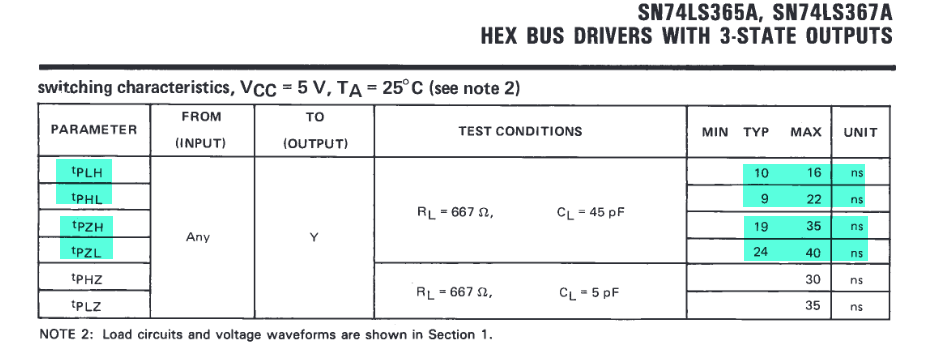
As can be seen, tPLH (propagation delay for a LOW to HIGH transition) is maximum 16ns. Whereas, tPZL (propagation delay for tri-state to LOW state) is maximum 40ns. Therefore, using a 2 buffer delay of the write signal will still not be sufficient to ensure the write data is stable! i.e. 2x 16ns < 40ns.
We could add one (or both) of the other LS367’s spare buffers, to create a 3 or 4 buffer delay. But, we will also need a way to deal with avoiding both the tri-state buffers and the 4464 DRAM data outputs creating their own driver contention, by them both driving the data bus at the same time!
So, with this in mind, and after a review of the different device datasheets, I came to the conclusion that a single octal tri-state buffer and a hex inverter would provide the best solution. After all, a 20-pin 74LS244 and a 14-pin 74LS04 added up to 34 pins, which is just 2 pins more than my original thought of using two 16-pin 74LS367’s. 🙂
Optimising Propagation Delays
A 74LS04 inverter has a typical propagation delay of around 10ns (max 15ns).
A 74LS244 Octal Buffer has a typical propagation delay from tri-state to LOW of 20ns (max 30ns), and tri-state to HIGH of 15ns (max 23ns).
Based on these timings, a two LS inverter delay of the write signal (20ns typical) may be just adequate to ensure the data is stable at the write pulse edge. As we have six inverters to play with, we could provide options for a two inverter, a four inverter, or even a six inverter signal delay.
But, for comparison, the 74HCT04 inverter has a typical propagation delay of around 14ns (max 25ns).
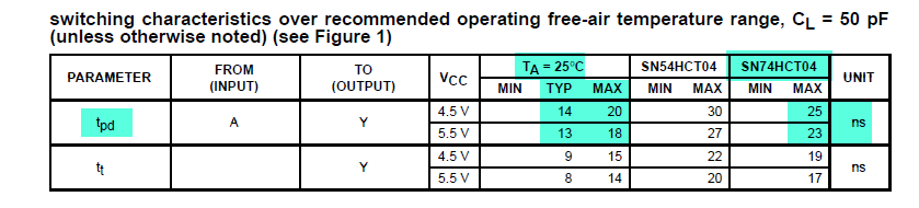
The 74HCT244 Octal Buffer has a typical propagation delay, not that dissimilar to the LS244, of around 19 – 21ns to transition from tri-state to an active output.
This actually looks to be providing a safer 28ns typical, using a two inverter delay. In addition, the 74HCT series are more commonly available and are often cheaper than the old school 74LS series, as well as also being available in a nice hobbyist friendly retro DIL thru-hole package.
Avoiding Bus Contention
In order to significantly reduce the chance of data bus contention, the 4464 DRAM also has a handy Output Enable Gate pin (pin 1), which when HIGH forces the output buffers into a high impedance state (tri-state). Something that the 4116 did not have, or need!
So, to minimise the chance of bus contention we can use the inverted write pulse to drive the 4464 output enable pin HIGH during the period when the 74HCT244 buffers are driving the data bus.
Conveniently, if we use the output of the first 74HCT04 inverter (in the write signal propagation delay chain), we will disable the 4464 output buffers typically 14ns after the VDP’s write signal is asserted, but typically around 5 – 7ns before the 74HCT244 outputs begin driving the bus. All sounds good.
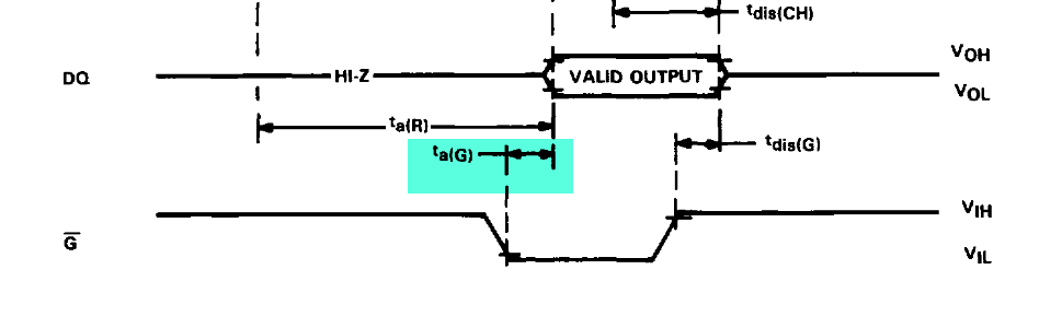
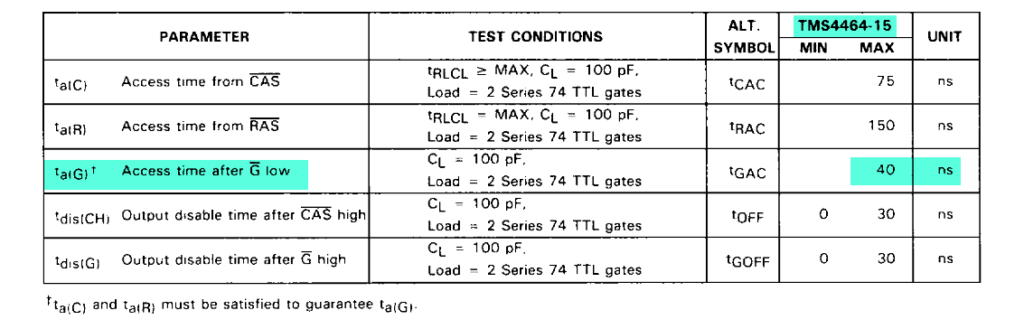
However, there is one other small timing constraint we should be aware of. That is the required delay time from the 4464 output buffers being disabled (output Enable pin HIGH), before data should be applied to the data I/O pins (i.e. tGHD). The TMS4464-15 datasheet specifies this as 30ns minimum!
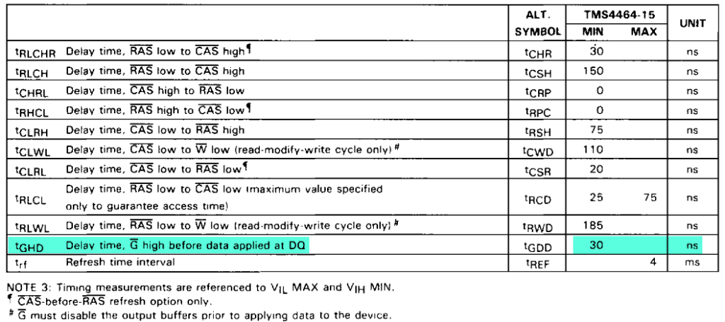
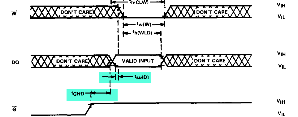
While viewing this timing diagram, it’s also of relevance to note that the valid input data setup time, before Write is asserted, tsu(D), is specified as minimum 0ns. i.e. There is no additional data setup time required prior to asserting the 4464’s Write signal.
Returning again to the minimum delay time from de-asserting the 4464 Output Enable, before data should be applied to the data I/O pins (i.e. tGHD). Clearly, with this specified as 30ns minimum (for the 4464-15), then the 5 – 7ns delay between de-asserting the 4464 output buffers and when the HCT244 outputs begin driving the bus, appears to be inadequate!
The solution to this is to simply move the HCT244 buffer Output Enable to be driven by the second stage of the hex inverter chain, instead of being driven directly by the VDP’s R/W signal. This is effectively adding two HCT04 inverter delays, or typically an extra 28ns added to the original 5 – 7ns extra HCT244 propogation delay. This satisfies the 30ns minimum tGHD spec.
Timing around the de-assertion of the HCT244 buffer Output Enable also appears to be compliant with this additional delay. The 4464’s delay until valid data output, after the Output Enable is again asserted ta(G), is specified as max 40ns. Although the minimum is not specified, I am comfortable that we’ll avoid data driver contention.
Summarising
So to summarise, my proposed updated “Retro” VRAM solution for the TMS9929A/28A VDP, would involve two 18-pin 4464 DRAM chips, a single 20-pin 74HCT244 Octal Buffer, and a single 14-pin 74HCT04 Hex Inverter.
Original 74LS series may also be used, but based on the satisfactory timing of the HCT devices, the general availability, the typically lower price, and the lower load and power of the HCT CMOS devices, HCT would seem the preferred approach.
This brings us to a total pin count memory chip solution of just 70 pins!
This satisfyingly delivers on my desire for an improvement over the 2010 Static RAM solution’s 102 pins (by a significant “32 less pins” improvement). This is great in terms of required PCB real estate and also the added ease of PCB routing. Or perhaps even just a welcome 32 less connections required if wiring this all up on a breadboard. 🙂
Testing the Alternative Retro VRAM Solution
My next step was to then capture my circuit idea into a KiCAD schematic.
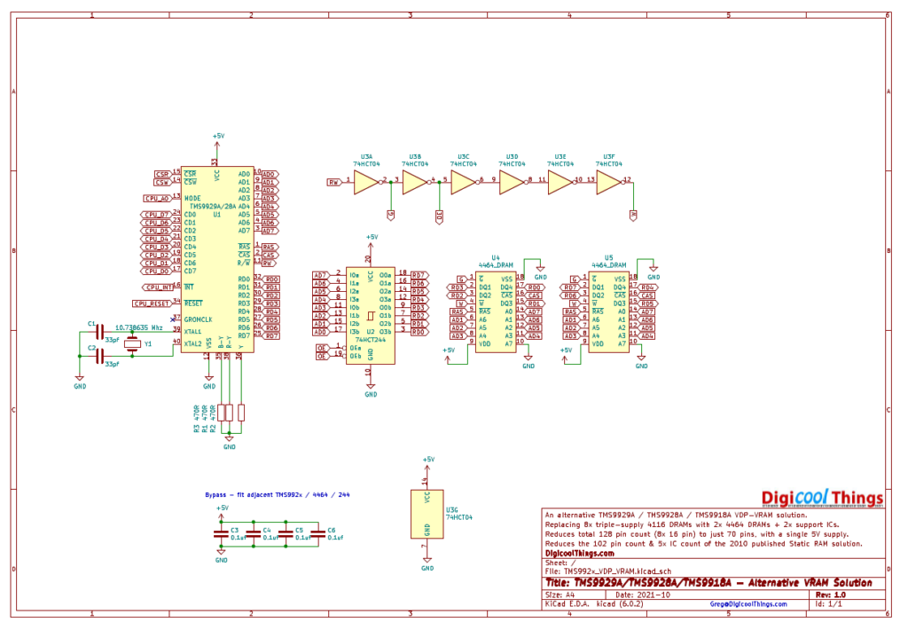
With a schematic done, it was time to pull out a breadboard and test the timings in practice and confirm the new design!
In order to thoroughly test the design, I connected up a TMS-RGB module for high quality video output, and used an Arduino to drive the TMS9929A.
An Arduino sketch was then written to test both the TMS9929A, and to perform multiple-pass varying bit pattern read / write tests on the full 16KB of VRAM.
Interestingly, I had previously made an Arduino based DRAM chip tester, but it occured to me that testing the DRAM via the TMS9929A actually provided a “real world access timing” based DRAM test, as compared to the practice of toggling the pins of a DRAM chip directly, via an Arduino’s GPIO, to simulate DRAM access and timing.
Success
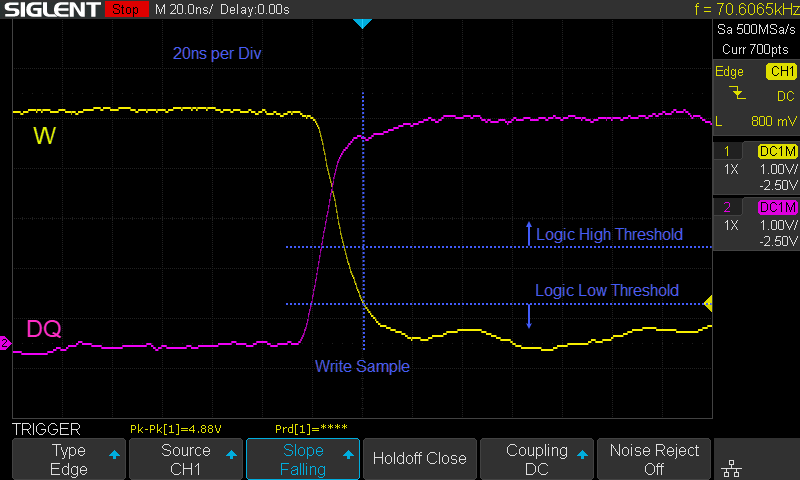
The circuit passed all tests without any issues, including tests across multiple DRAM chips with various common speeds of 100ns – 150ns (i.e. -10, -12 and -15 suffixes). I infact used the circuit to test my entire stock of 4464 DRAM chips.
I walk-through the Arduino sketch and demonstrate the resulting TMS9929A output in my Youtube video.
As a final note, below I’ve annotated a scope trace of the captured actual Write pulse HIGH-to-LOW transition, relative to a LOW-to-HIGH input Data transition. This shows around an 18ns Data setup time, from the HIGH Data transition, to the LOW Write transition, on my breadboard test setup.
Next Step
With my Alternative / Improved Retro VRAM Solution circuit tested and confirmed, I’ll next create a TMS992xA VDP board for my new Minimalist Europe Card Bus (MECB) design. This will then allow me to easily experiment with my TMS9929A with whatever 8-bit CPU or memory map that I choose.
Links
TMS9929A VDP on GitHub – VRAM Solution Schematic / Arduino Test Sketch
Discussion
Discuss this post in the Forum