
This post follows on from my earlier Minimalist Europe Card Bus posts and videos. For MECB, to date I’ve designed and built a Backplane, a Prototype card, and a TMS9929A Video card. The next logical step is to create my first CPU card.
My MECB modular design project originated from the rediscovery of my Motorola 6809 wire-wrap Eurocard based CPU board, which I’d designed back in the early 1980’s. You can watch my earlier posts / videos exploring this board, if you’re interested in more detail.
As a result, it’s not surprising that I’d create my first CPU card around my favourite retro 8-bit CPU, the 6809. Effectively, my MECB design journey, was really kicked-off by me taking my original 6809 wire-wrap board, and updating it into a modular PCB based design. Also, implementing the flexibility required to support experimenting with different system configurations and memory maps.
Essentially, the original wire-wrap CPU board is being split into a modular two card design. Putting the CPU and Memory onto one card, and the I/O onto a second card (or cards). These cards are then reunited by the MECB backplane, where other cards can then be added for experimenting with. For example, the previously built TMS9929A Video card.
Whereas the original 80’s wire-wrap CPU board had only 2KB of RAM, and 4KB of ROM, the new CPU card will have on-board a full 64KB of RAM, and a generous 32KB of ROM. This allows the flexible chip select logic to be configured however you decide, for allocating this available memory into the CPU’s 64K address space.
For example, one relatively common memory allocation might give the first 56K of address space to RAM, and the top 8K for ROM.
You could even choose to exclude the on-board memory, if, for example, a paged memory card was later added. There’s plenty to play with!
So let’s take a look at the KiCAD schematic.
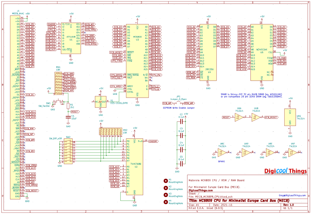
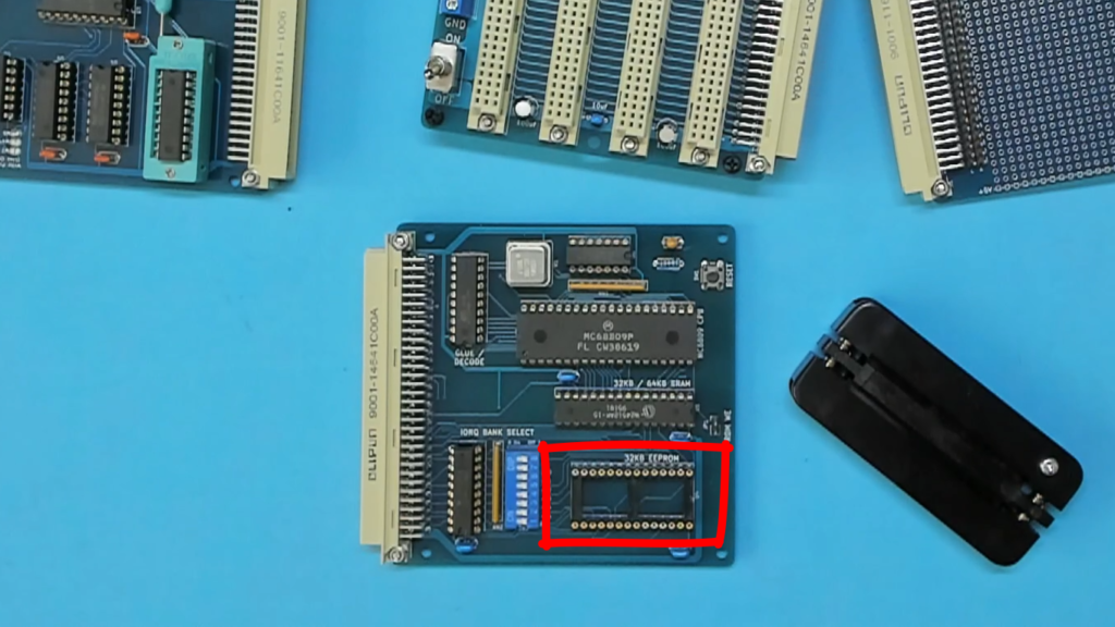
As can be seen, the CPU card is dominated by the CPU chip, a single byte-wide static RAM chip, which can either be a 64KB 32-pin skinny DIP, or a pin-out compatible 32KB 28-pin skinny DIP. Also, we have a single 32KB 28-pin FLASH ROM.
In addition, we have a standard crystal oscillator, a Schmitt trigger based reset circuit, and our flexible glue logic PLD chip.
Finally, we have a comparator and 8-way DIL switch, to allow selection of a memory mapped I/O address space, to exist in any 256 byte page of the 64K address space. This implements the MECB Bus I/O Request signal (or IORQ).
Note that as per my original wire-wrap board, this first CPU card design is based around the original internal clock version of the 6809 chip. That is, the non “E” suffix version of the CPU.
This was simply in basing the design on my original 80’s design, and is also due to me having several of these internal clock 6809 chips in my old parts storage.
But, you may have noticed from a couple of my recent posts, that I’ve had some difficulty finding a source for non “E” suffix 6809 or 6309 CPU’s. Even the chips I ordered, which were clearly marked as non “E” variants, turned out to actually be re-marked “E” suffix External clock CPU chips.
Because of this, I will be making my second CPU card design, an External clock 6809E (or 6309E) CPU card.
This will effectively be the same design, just with the addition of the required quadrature clock generator, and perhaps some other updates. But otherwise, it will be functionally equivalent to this non “E” variant CPU card design.
But, before I get ahead of myself, let’s return our focus to this initial 6809 (or 6309) CPU Card design!
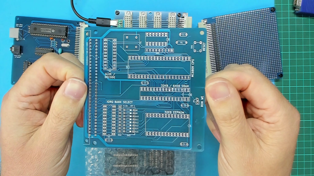
So let’s take a look at the PCB layout.

As per my previous MECB related posts, I created this KiCAD project by using the standard MECB KiCAD template, that I had created earlier. This sped up the process significantly, by letting me start-off with a pre-defined PCB, with mounting holes, and with the bus connector etc., already in-place.
As you can see, the rest of the PCB layout came together relatively nicely, with plenty of space available on the MECB standard 100mm square PCB size, to allow for relatively easy trace routing, with a simple and cost effective 2 layer board.

These initial prototype PCB’s were ordered from JLCPCB, and here’s what they look like.
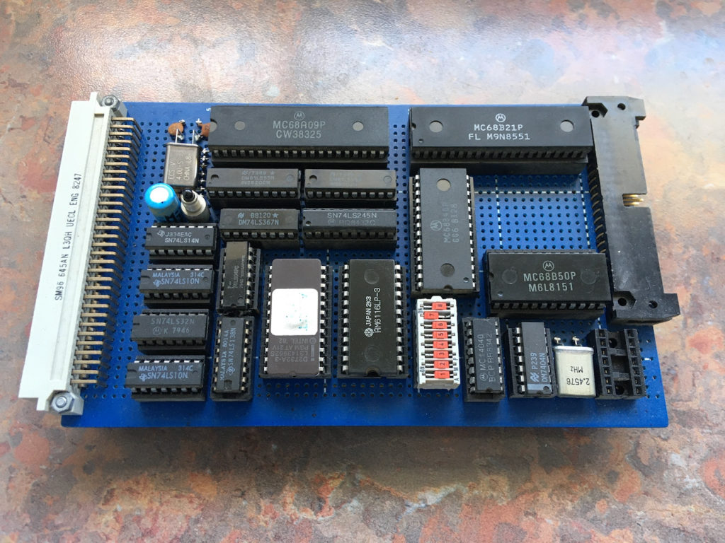
I assembled my first PCB prototype, starting off with the resistor and capacitors, as well as the two Single In-Line resistor packs.
Then I soldered in the IC sockets, including an 8-pin IC socket that I’ve modified for the Crystal. 4-pin Crystal sockets are relatively expensive, but you can modify a regular round-pin IC Socket for the purpose, by just popping-out the centre 4 pins, leaving just the 4 corner pins. I then also soldered in the ROM Write Enable 2pin header.
Then, the 8-way Dual In-Line switch and the momentary Reset switch.
Finally, the male DIN 41612 MECB bus connector, which is secured in place with a couple of 10mm M2.5 bolts.
I then got some of the IC’s inserted. First the Hex Schmitt-Trigger Inverter. Then the 74HCT688 8-bit Comparator. Then a 64KB Static Ram, and our internally clocked 6809 CPU chip. Lastly, for now, I used a 4Mhz crystal oscillator to run the CPU at 1Mhz.
With just the PLD and ROM chips remaining, next I defined and programmed the PLD chip.
For a CPU card, the PLD chip usage is a little modified, as compared to the standardised PLD pin usage that I had outlined in an earlier post.
The standardised PLD pin usage, described in the earlier post was specifically for PLD usage on Peripheral cards, where the bus signals are all acting as PLD inputs available for generating up to three Peripheral “Chip Select” outputs.
In the case of a CPU card, the PLD is still used for generating flexible “Chip Select” outputs, but, for a CPU card we also use the PLD for generating some of the bus signals which originate from a CPU card.
So let’s take a look at the PLD chip configuration.
Firstly we define the PLD input pins.

For the CPU card we are using 10 pins for inputs.
First we have the active low I/O address output from the 74HCT688 8-bit comparator.
Then we have the CPU’s E and Q clock signals, and the CPU’s Read/Write signal.
And finally we have the top six lines of the Address bus. This allows the PLD to select memory address space down to 1KB boundaries.
Next we define the PLD output pins.
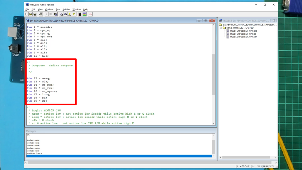
For the CPU card we are using the remaining 8 I/O pins as outputs.
These include the usual pin 14, 15 and 16 allocations for up to three chip select outputs.
For this card we will define these for the ROM and RAM chip select, with one unused spare.
The remaining 5 output pins are used to generate the MECB bus signals that originate from a CPU card.
These are, the memory request, clock, I/O request, and the separated read and write signals.
With the pins assigned, we then created the simple logic equations used to define the outputs, based on the status of the relevant input pins. I summarised all of this in the source comments.

Firstly, the memory request output is active low, and is asserted when the I/O address signal is high (i.e. not active), while either the E or Q clock signals are high.
Then the clock output is set to follow the CPU’s E clock signal.
The ROM chip select is an active low output and is asserted when memory request is asserted and address lines A15, A14 and A13 are all high. This equates to the top 8KB of memory address space from 0xE000 to 0xFFFF.
The RAM chip select is an active low output and is asserted when memory request is asserted and address lines A15, A14 and A13 are not all high. This equates to the bottom 56KB of memory address space from 0x0000 to 0xDFFF.
The spare chip select pin is not connected on the PCB, but I’ve just allocated it as an active low output when I/O request is asserted.
i.e. It just follows the I/O request output pin.
We then have the I/O request output pin, which is active low, and asserted when the I/O address signal is low (i.e. active), while either the E or Q clock signals are high.
As you’ll note, this is the opposite to the memory request signal. So, either the memory request or the I/O request signals are asserted during a high E or Q clock signal, depending on the state of the I/O address signal that defines the 256 byte page of the address space that we have allocated (via the 8-way DIL switch) for I/O address device use.
Finally we have the active low read and write output signals, which simply split the 6809 CPU’s combined R/W signal, and asserts only during the E clock signal’s high period.
With the PLD definition completed, I then compiled the definition and programmed the PLD chip with the output .jed file.
If you’re interested in how this was done, then please view my earlier post where I discussed in more detail the Address Decode / Glue Logic ATF16V8 use and programming.
With the PLD chip now inserted into the PCB, this just leaves the ROM chip.
As we don’t yet have any I/O, a standard monitor ROM isn’t going to be of any use to us, as we currently have no serial interfaces to allow talking to the CPU card.
Instead, for the initial testing of this card, my plan is to just write some ROM code. Either something I can monitor (to confirm all is operational), or preferably, to get the CPU doing something visual with my TMS9929A video card.
But, this post is probably long enough already, so we’ll leave the code and final testing for a part 2.
UPDATE: Part 2 can be found here