
This post follows-on from my previous post, where I presented and assembled my first prototype PCB for a 6809 CPU card, for the MECB bus. The first part concluded following the PCB assembly, but prior to testing for successful operation of the CPU card.
Now, for Part 2, we will write some code for testing the CPU card, configure the address decoding, and also perform troubleshooting to determine why the CPU card Failed to work first time!
Part 1 can be found here
Testing Approach
As we have yet to build a MECB I/O card, we don’t currently have a serial interface available. We in fact don’t have any I/O on our CPU card.
We do however have our TMS9929A Video card, which we built and successfully tested earlier.
So, in order to test the CPU card, my plan is to do the modern equivalent of what we hobbyists had to do, when testing new CPU designs, back in the early days. Only, a whole lot easier than we had it back then!
When I built my first microprocessor based design, we didn’t have computers. So, the initial code was “hand assembled” on paper, with a pencil.
That’s right, we didn’t have Computers, or Assemblers. So, we wrote raw machine code, with pencil and paper.
First writing down the CPU’s instruction mnemonics, and then manually translating these into the hex byte opcodes and operands, needed by the CPU. This also included having to manually count back (or forward), to calculate branch offsets.
We then had to manually enter each byte into our homemade standalone EPROM programmer.
Needless to say, it was a very tedious and time consuming method of program development, with plenty of opportunity for introducing human error, to further complicate debugging.
Although, it’s fair to say, when you eventually created a successfully working solution, it was highly rewarding!
Today we have the huge advantage of computers, enabling easy editing & saving of our source code. Also, Cross Assemblers for automatically generating the required hex object code. As well as cheap and highly capable PROM programmers.
In addition, we have cheap single 5v FLASH ROM’s and other electrically erasable ROM’s, so we no longer have to use UV Erasers for our EPROM’s, or require multi-voltage power supplies for for the likes of the early triple-supply 2708 EPROM, that I first programmed.
The Plan
So, the plan is to write some assembly code from scratch, assemble it, and program the assembled code into the flash ROM for testing. Effectively, the same process we used in the early days, just a whole lot easier now than it was back then.
Since I’ve already tested the TMS9929 VDP card with some Arduino code, the best way forward is to replicate this existing test program onto my 6809 CPU card.
Basically, by effectively porting the existing code across, to create a ROM friendly 6809 Assembly Code version.
I’ve skipped the VDP VRAM testing that was included in the Arduino code, as that VDP test has already been done by the Arduino, and our goal now is simply to test the 6809 CPU card!
So, the approach I’ve taken is to re-write each existing routine, that I’d developed for the Arduino, into an equivalent 6809 subroutine.
Implementation

Firstly, I define the code entry point as address $F000, which puts the code at the beginning of the top 4K of the address space.
Then I define the address of the VDP chip.
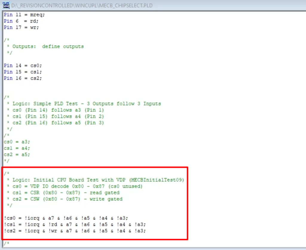
As I’d noted in the header comments, I decided to use an IORQ based VDP address allocation.
So, the CPU card’s DIP switch will be used to allocate the $E0 page (i.e. $E000 to $E0FF) to be the memory mapped IO address space, and the VDP card’s address decode will be allocated as the IO space $80 to $87.
Therefore, we equate ‘VDP’ to be the $E080 base address, with ‘VDP_ VRAM’ and ‘VDP_REGISTER’ assigned as the two VDP addresses we will be accessing.
Next we have the main entry point of our code, which starts off with the reasonably standard reset initialisation of the 6809’s system stack pointer (so we can call subroutines), and the usual initialisation of the Direct Page register.
Before looking at the rest of the mainline code, let’s talk about the subroutines. As mentioned earlier, I’ve simply rewritten the VDP access routines that I’d originally implemented in Arduino code. I’ve named (or labelled), the 6809 subroutines the same as the equivalent Arduino routines for easy association.
The code is all relatively straightforward, and (as usual), I’ve clearly documented the code.
I’ll mention that three of the Arduino equivalent routines are included here only for documentation purposes.
As their 6809 equivalent is just a single store or load instruction, clearly we won’t bother calling a subroutine just for this, as the store or load instruction itself is quite self explanatory and would therefore just be coded in-line.
These are the readStatusByteVDP, readVramByteVDP, and the writeVramByteVDP routines.
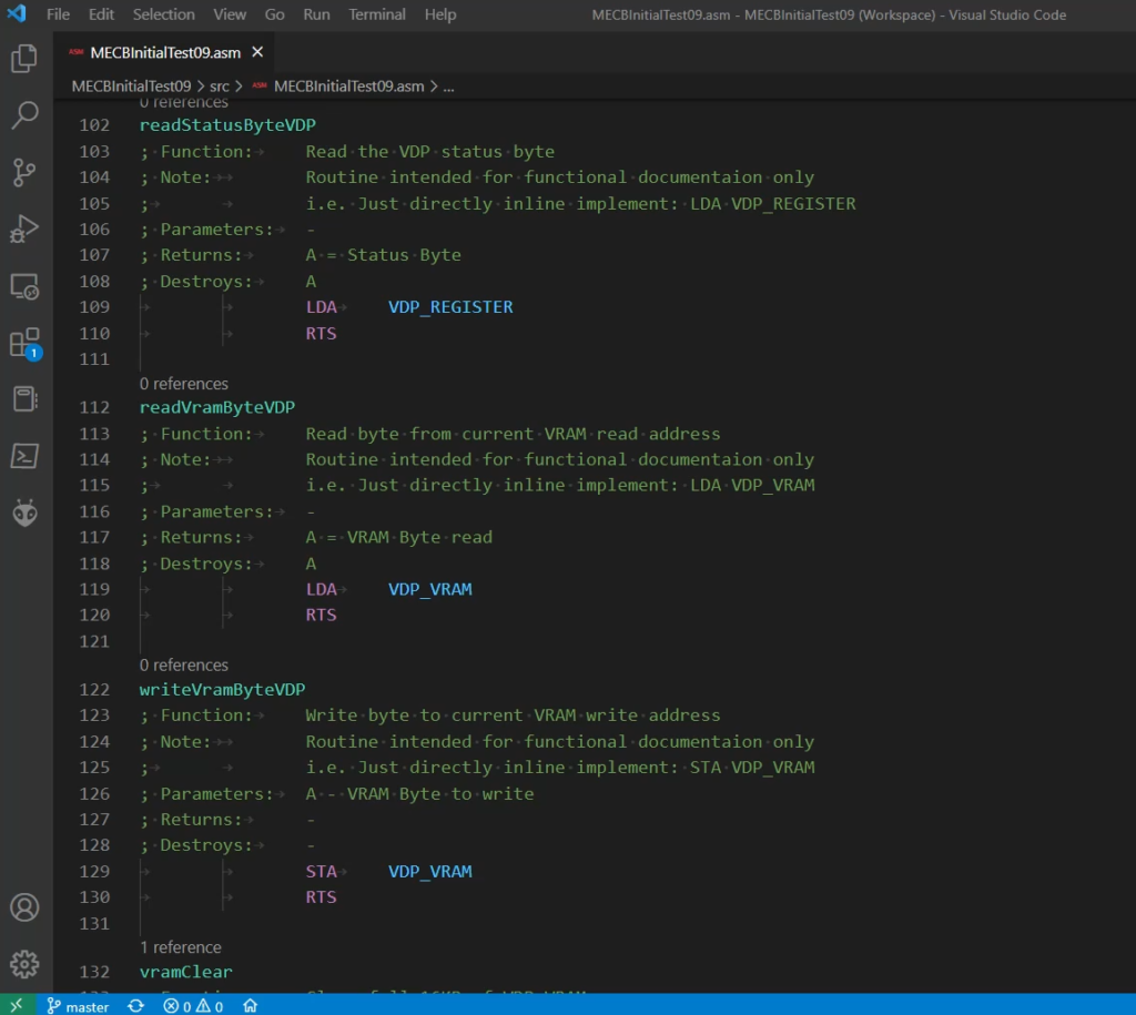
The vramClear and the vramSetup subroutines then follow, which are again quite self explanatory. Both of these routines involve small loops.
Finally, we have two delay routines. The first being a simple 1ms delay, and the second being passed a parameter to specify the number of millisecond delays we want.

As you’ll note from my comments, without a timer available, these delays are achieved via a simple loop, with each instruction execution cycle count noted, and the approximate 1ms subroutine time having been calculated based on a 1Mhz clock.
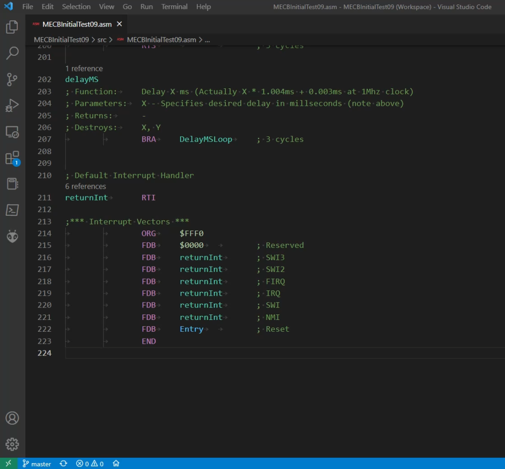
Then, at the end of the ROM, from addresses $FFF0 to $FFFF, we have our standard 6809 interrupt vectors.
Of which, the Reset vector points at our mainline entry address, with the rest of the possible interrupts pointing at a default interrupt handler, which just immediately returns.
And that ends the code.
Returning to the mainline code, we first setup the VDP registers. Then we clear the VRAM, and setup the VRAM tables.
Finally, we loop forever, simply changing the VDP backdrop colour every two seconds (approximately), just as we did with the Arduino based VDP card test.
Note, this code hasn’t in any way been optimised, as for card testing purposes it makes more sense to keep it simple.
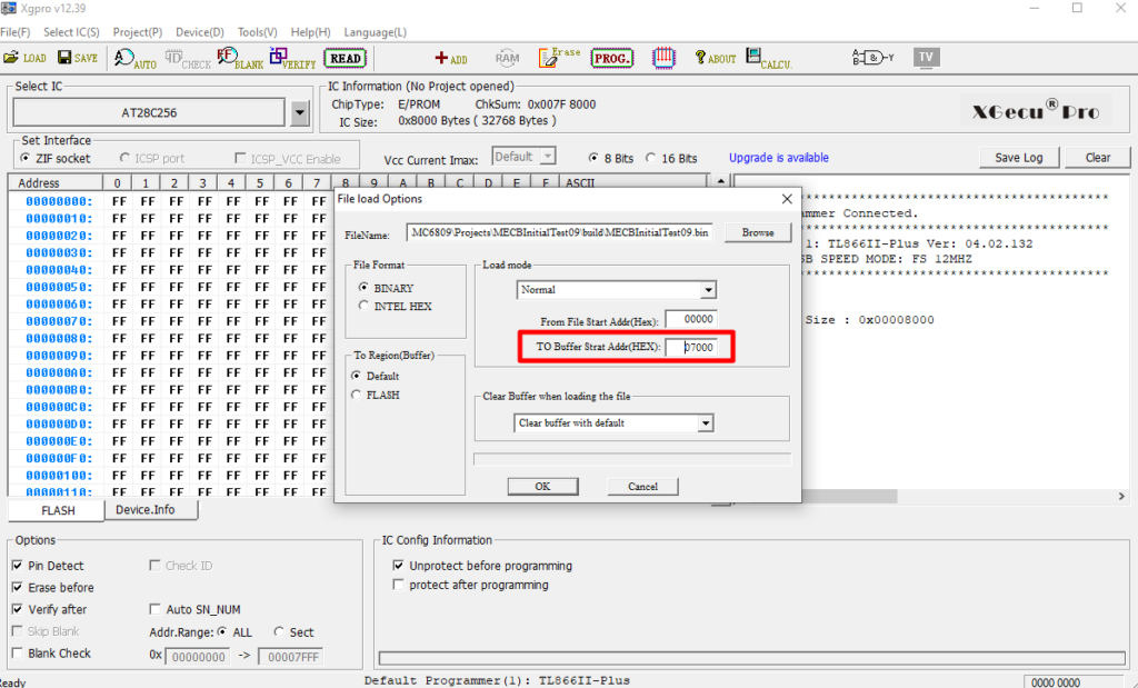
Assembling this code into a raw .bin file, allows us to program our 28C256 32KB ROM.
The resulting bin file is 4KB in size, intended to be located in the top 4K of the address space. i.e. From $F000 to $FFFF.
So, we load this into the programmer at buffer location $7000, which equates to the top 4KB of our 32KB ROM chip.
Once programmed the ROM was then inserted into the ROM socket on our CPU card. In addition to this, we set the CPU card’s 8-way DIP switch to indicate we are allocating the $E0xx page for the memory mapped Input / Output space.
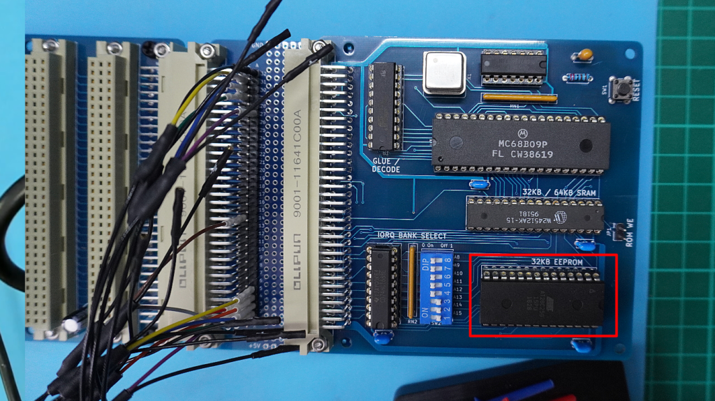
Finally, we need to update the VDP card’s address decode PAL logic, to enable the CSR and CSW to be asserted for the IO address block $80 to $87.
With the updated PAL chip re-installed back into the VDP card, we are now ready to apply power and see if our test is successful.
Failure!
This is where it gets interesting. You see, when powered-up, the display just stayed blank! i.e. The initial test Failed!
To be honest, I was pretty happy with this. After all of my previous MECB card design tests worked first time, I was actually keen to do some fault finding!
So this is what lead to me hooking up my Logic Analyser, in order to help find where I’d gone wrong.
In a way, using a logic analyser does feel a bit like cheating, as I have distinct memories of having to sort out test failures (like this), in the early days, with nothing more than a Multimeter and a simple Logic Probe.
These were the only tools available to me, and were only good for for basic tests and giving my vague clues as to where the problem might be.
Actually solving the problem generally came down to going over every detail with a fine-tooth comb, re-checking everything, until you were able to isolate where either your coding, your design logic, or a component had failed.
These days, a Logic Analyser makes zeroing-in on the fault so much easier. And, just like we now have Computers and Cross Assemblers to make life so much easier developing our CPU code, I’d be silly not to take advantage of my modern fault finding tools for debugging my retro designs.
So here’s the output of the Logic Analyser, triggered by the rising edge of the Reset signal.

As you can see, I’ve labelled the 16 signals I’m capturing.
This is a 16 channel logic analyser, so I’m not able to capture all the system signals, so I’ve omitted the address bus.
Instead we are capturing the Data Bus, Reset (for our trigger), then the bus Clock, MREQ, IORQ, Write, Read, and the Chip select signals for both the RAM and the ROM.
First, we can see that we are getting no activity on the data bus. With constant 00 bytes.
After Reset returns high, we should be seeing the Reset Vector being read from the ROM.
We can see the ROM chip select is being asserted. BUT, what is immediately apparent is that the Chip select signals do not look right!
These signals should be asserted (Low), when MREQ is low. Instead, both the ROM and RAM chip select signals are being asserted when MREQ is inactive (High).
So, this gives us an obvious clue, in that it appears we have an error in our CPU card’s PAL logic.
I went over the original WinCUPL source for the CPU PAL logic, in the previous post / video.
Now that we have the vital clue from our logic analyser, the logic error I’ve made is plainly obvious.
For both of the active low ROM & RAM Chip Select signals I am testing for MREQ to be High, instead of requiring MREQ to be asserted (Low) .
So, simply prefixing MREQ with a Not, for both ROM & RAM Chip Select, will resolve this logic error.
While I’m at it I can see a similar logic error for the unused spare Chip Select. This was intended to follow IORQ, but once again I had forgotten the Not prefix, so the active low output will follow the active low IORQ signal. Not that it really matters, as this output is unused.
So with these changes made, I’ll re-compile the code and re-program the CPU card’s PAL chip.
Success?
With the updated PAL chip re-installed back in the CPU card, I then power-up to see if we now have success, and take a look at an updated sample from our logic analyzer.

Above is the updated sample from our logic analyser. Now we see that the Chip Select ROM signal looks more appropriate. And, importantly, we can now see the expected activity on the Data Bus.
We can see the F000 reset vector being loaded, and the code being read and executed. Scrolling along a bit, I can also see the return address for the first subroutine call being written to the stack in RAM, and also, the first byte being written to the VDP, via our IORQ.
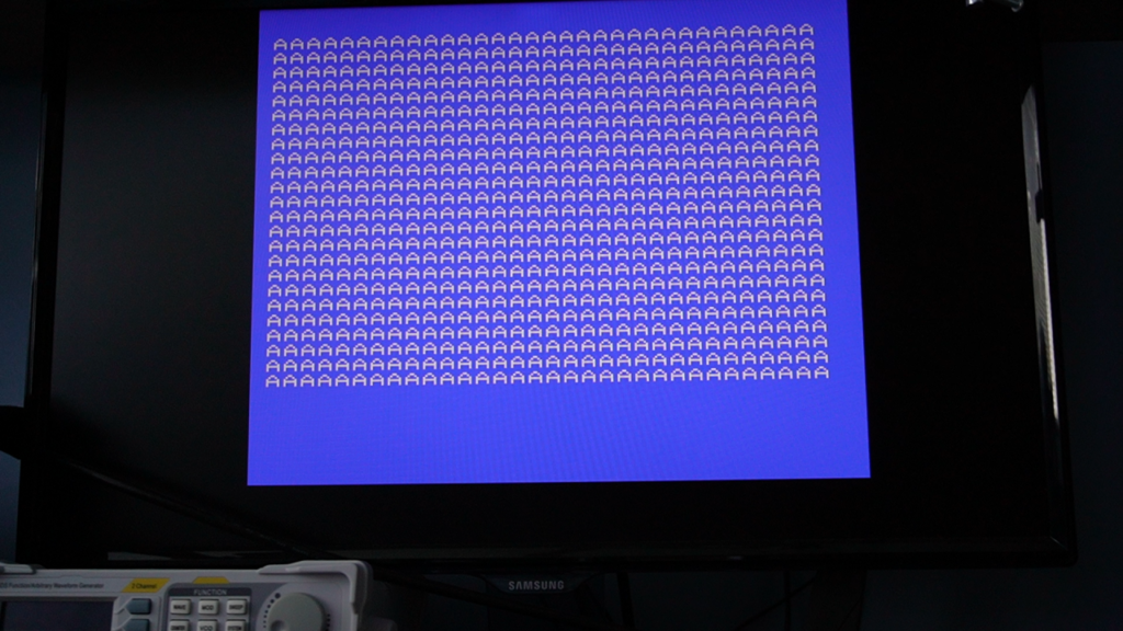
Finally, looking at our display, we have Success!
Conclusion
We now have our 6809 CPU card successfully working with the VDP card, running our VDP display code, displaying what we previously saw from our Arduino driven VDP card test.
Awesome, we’re now well on our way to a standalone MECB system… Once we add an I/O card. 🙂
Follow-up
Following this post & video, feedback lead me to improving the clarity of the WinCupl logic code. Specifically, inverting the Active Low signals at the pin declarations, so that all logic equations are now solely based on positive logic.
This improved logic clarity should avoid making the same logic error again in the future.
I have also made some changes and optimisations to the 6809 Assembly code.
Both of these changes are available via the main MECB GitHub repository (see link on the main MECB page).