
This post / video follows on from my earlier Minimalist Europe Card Bus posts and videos.
My original (version 1.x) MC6809 CPU Card required an original internal clock 6809 (or 6309) CPU.
After trying to source more CPU chips, it became clear that although External clock variant 6809E CPU’s were readily available, the original internal clock variants (non-E suffix), were hard to find.
For this reason I decided to re-design my 6809 CPU Card to now support either the internal or the more commonly found External clock CPUs.
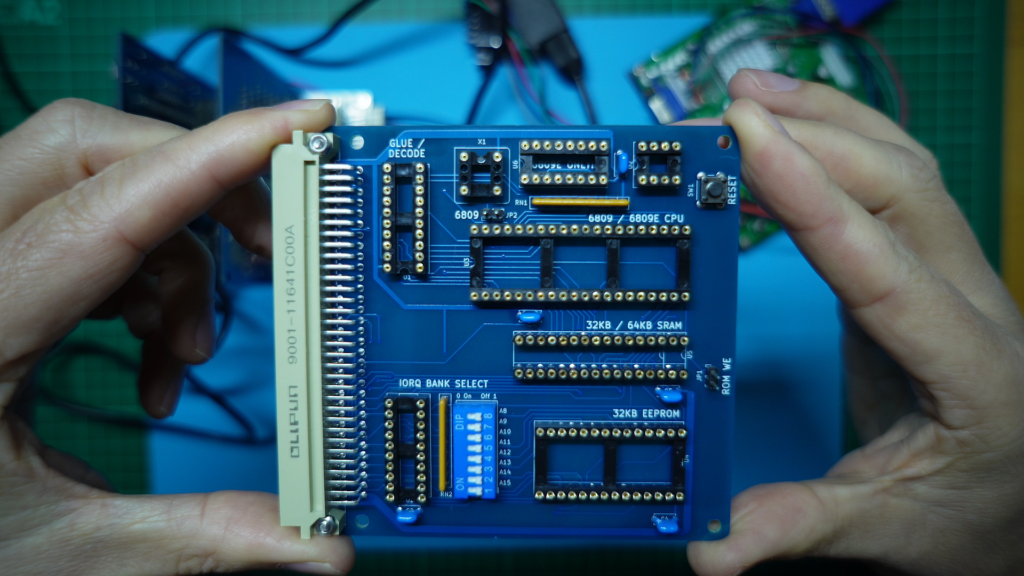
This is my 6809 / 6809E CPU Card v2.x.
Join me as I walk through the schematic and PCB changes, and then assemble and test my first card.
This journey also includes a good lesson for any young circuit designers’ to take note of, as we encounter some design fails along the way!
You can also refer to my earlier posts covering my difficulty attempting to source original internal clock 6809 or 6309 chips, where I received only incorrectly re-marked chips. You can view these post here and here.
On the basis of this, I decided I should create an updated 6809 CPU Card design. One which would be compatible with either the internal or the external clock CPU chips.
This requires the addition of a circuit for an external quadrature clock generator, and also a jumper to allow disconnecting the crystal oscillator’s direct connection to the CPU itself.
With this new design, by inserting the jumper, but not the clock generator chip, the board is compatible with the original internal clock 6809.
Alternatively, by removing the jumper, and inserting the clock generator chip, the board is now suitable for the easier to find external clock 6809E CPU.
While making these changes, I also took the opportunity to update the CPU card’s reset circuit, as I described in more detail in my previous post / video, titled “Optimising our Retro CPU Reset Design“.
The result is my “Version 2” 6809 CPU card, which now supports either the Motorola 6809 or Hitachi 6309, as well as either the Motorola 6809E or Hitachi 6309E external clock processors.
I’ll now present the updated schematic, updated PCB design, and then I’ll assemble and test my first PCB.
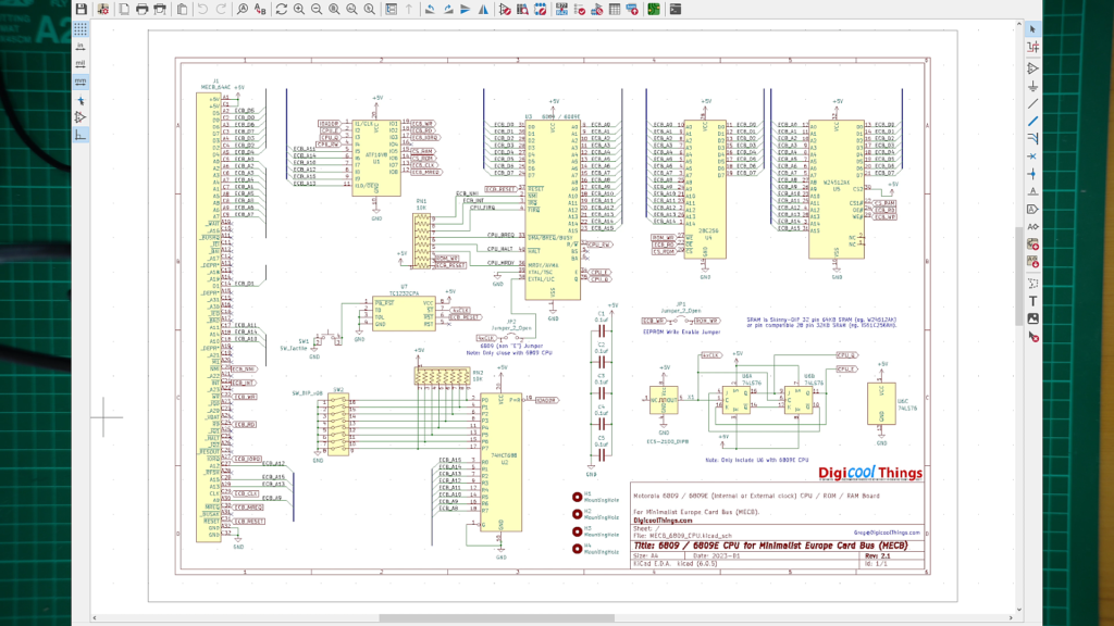
Firstly, as you can see, based on some earlier feedback, I’ve updated my KiCAD schematic to now utilise bus connectors, to make the circuit a little easier to follow.
Other than this, the changes to the earlier design are basically:
- The inclusion of the quadrature clock generator circuit, based on a dual J-K flip flop.
- A CPU jumper, to allow disconnection of the clock signal from the CPU chip, for 6809E CPU’s.
- And, the simplification of the reset circuit, to now utilise the TC1232 8-pin Dual In-Line “Microprocessor Monitor” chip.
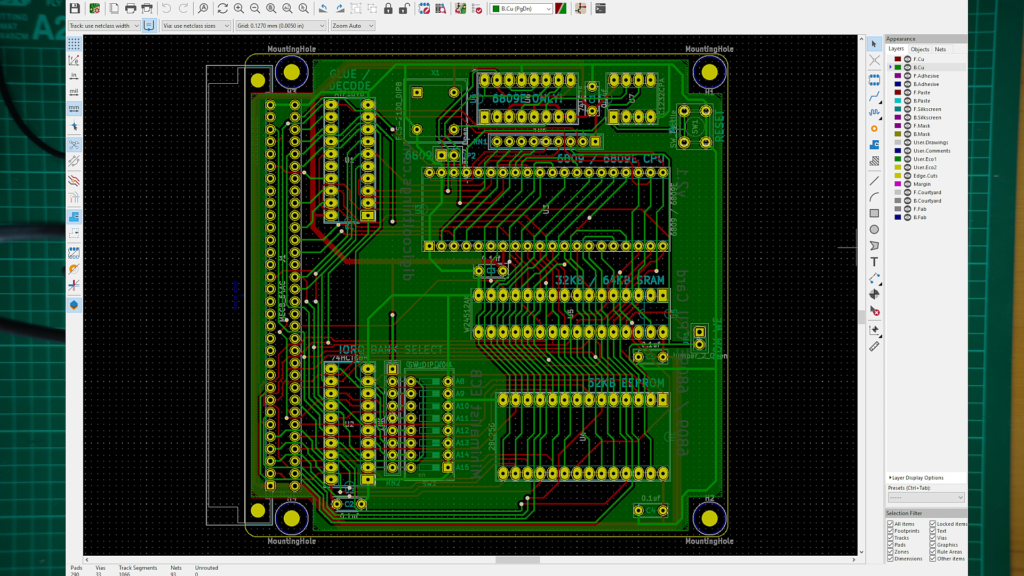
You can see that the PCB layout hasn’t changed much. Basically, because the clock generator and the updated reset circuits both fit in the same PCB space that was previously required for just the original reset circuit. Nice!
Let’s take a look at the new PCB, and get the first one assembled.
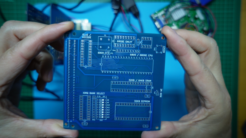
For assembly I started off with the bypass capacitors, and the two Single In-Line resistor packs.
Then I soldered in the IC sockets, including an 8-pin IC socket that I modified for the Crystal.
4-pin Crystal sockets are relatively expensive, but, as I did previously, when assembling my earlier 6809 CPU board, I modified a regular 8-pin round-pin IC Socket for the purpose. By popping-out the centre 4 pins, leaving just the 4 corner pins.
I then also soldered in the ROM Write Enable and the 6809 CPU 2-pin headers.
Then, the 8-way DIL switch and the momentary switch for the Reset.
Finally, the male DIN 41612 MECB bus connector, which is secured in place with a couple of 10mm M2.5 bolts.
With the board assembly completed, it was time to get some IC’s inserted.
As we have tested “known good” IC’s on the original v1.x MC6809 CPU card, I decided to just move these over.
Firstly, the 74HCT688 8-bit Comparator. Then a 64KB Static Ram, and then our internally clocked 6809 CPU chip. Next, the 4Mhz crystal oscillator to run the CPU at 1Mhz.
I leave the clock generator chip uninstalled for now, as we’re first testing the new v2 CPU Card with the same original internal clock 6809 CPU that we used in the earlier CPU card.
Finally, I also just move across the programmed PLD and ROM chips, which we had previously used for configuring and testing the earlier v1 CPU card.
Next we added our new TC1232 8-pin DIL chip, for our compact “no additional external components” Reset solution.
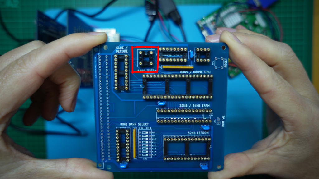
The last thing was to insert the jumper to feed the crystal oscillator clock directly to the internal clock 6809 CPU.
With the v2 CPU Card now ready to go, we then inserted it into our backplane, alongside the TMS9929 video card, for its first test.
So, we applied power to see what we got!
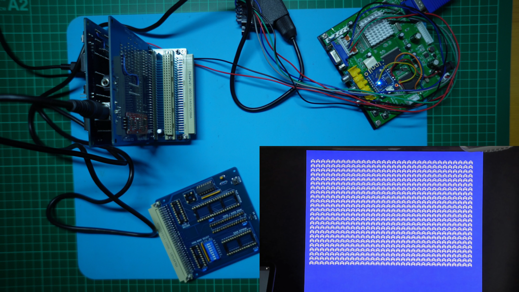
As hoped, we have the same video display test output. So, we have SUCCESS with using the internal 6809 chip, replicating the function of the original v1 CPU card.
Next, we want to try the CPU card configured for the more common 6809E external clock CPU.
So first we take out the internal clock CPU, and also remove the 6809 CPU jumper.
Then we insert the 74LS76 J-K flip-flop chip, for the quadrature clock generator.
Finally, we insert a 6809E CPU. In this case I have the Hitachi 63B09E chip that featured in an earlier post as an incorrectly re-marked chip from AliExpress, that some rubbing revealed was actually an External clock variant, instead of the internal clock version it was marked as.
With new chips mounted we again applied power to see if we also have External clock success.
Unfortunately this test was a FAIL.
As the internal clock CPU test was successful, this points us to the External clock generator as the most likely cause of the failure.
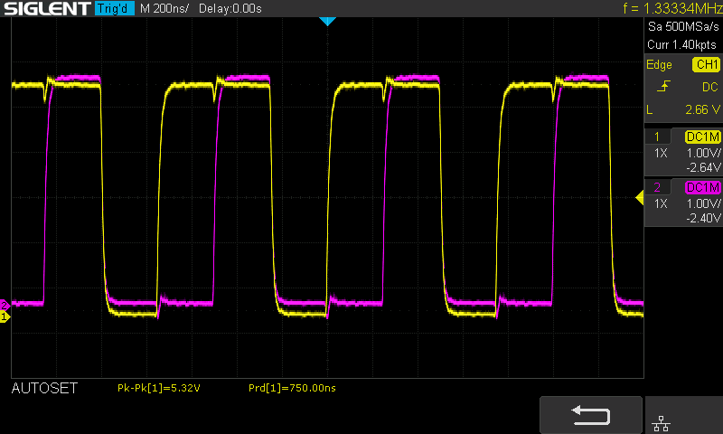
Hooking up the scope verified that we were getting an unexpected quadrature clock signal. Instead of a 50% duty cycle 1MHz clock, we are seeing a 1.33Mhz 33% duty cycle clock. Not what we want!
I next swapped out the 74LS76 flip-flop, and also tested the chips to ensure it’s not a faulty part that’s causing the issue.
Before continuing, I’ll just say that this is turning into a good lesson for young design engineers.
I’ve been doing this for a long time, so I should know better. But, the reality is that, when you’ve been doing this for a while you can easily get a bit over-confident and take shortcuts.
To explain what I mean, the Quadrature clock circuit I used originated from the official Motorola datasheet for the 6809E. The same circuit is also replicated in the official Hitachi datasheet for the 6309E.
Here is the circuit as shown on page 12 of the Motorola 6809E datasheet.
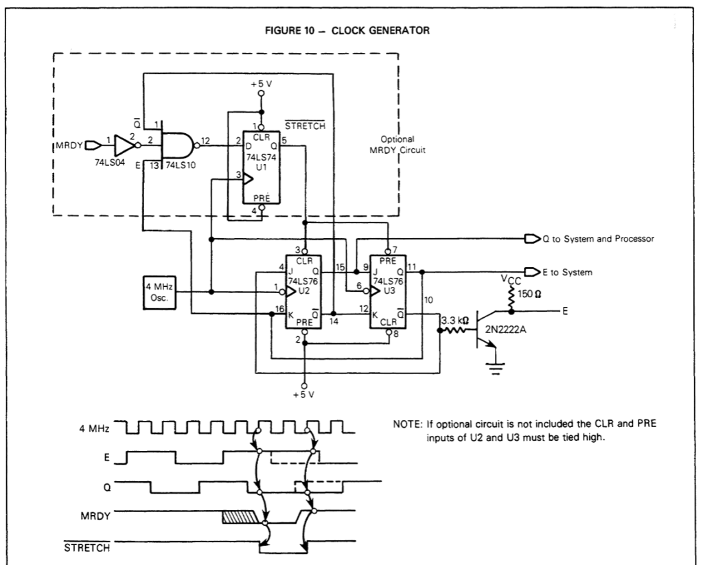
Note that the “Memory Ready” function of the circuit is optional, and if not used, the Preset and Clear inputs of the 74LS76 J-K flip-flop should all be tied high, as I did.
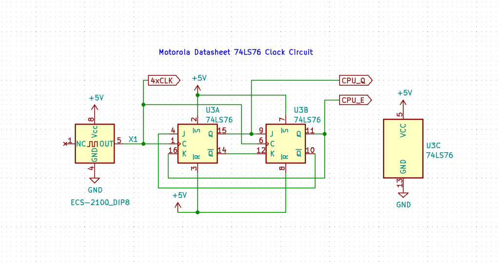
Reviewing the Dual J-K Flip Flop circuit, it certainly looks like a reasonable circuit for generating an appropriate divide by 4 quadrature clock.
So, this is the lesson:
Even though we are using an officially recommended circuit, a good designer should analyse the circuit further, and (ideally) also verify that the circuit actually functions as expected, before going ahead with designing and manufacturing a circuit board!
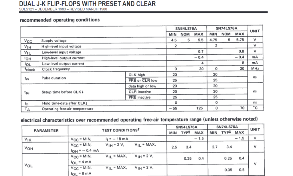
My first observation is that the circuit specifies a 74LS76, whereas my flip-flop chips are 74LS76A. Referring to the datasheet, the ‘A’ suffixed variant has a subtle difference.
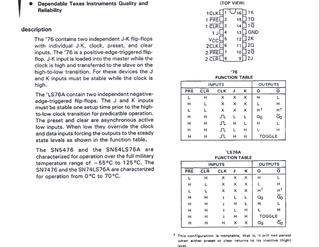
The non-A variant states that the J-K input is loaded while the clock is high and transferred on the high to low clock transition. The J & K inputs should remain stable while the clock is high.
Whereas, the A variant is simply noted as negative edge triggered.
Now, I had ordered 74LS76N chips from AliExpress, but I actually received 74LS76AN chips.
I suspect, as the 74LS76 device is no longer in production and is therefore a recovered chip, it will be difficult to find non-A variants, as the AliExpress suppliers probably don’t recognise the difference.
Despite this difference, after I further studied the datasheet, I would have still expected the 74LS76A to function in this circuit.
Here’s my reasoning why.
Firstly, I’ve put together this diagram to show the expected output of the circuit, together with the output that we are actually getting.
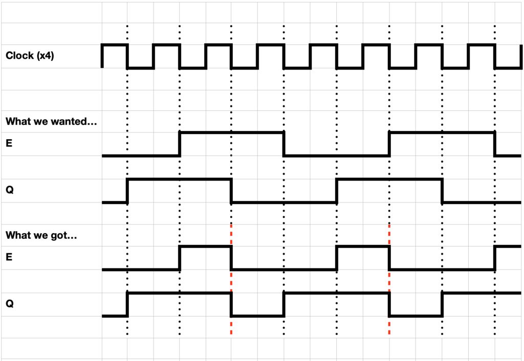
Analysing the output we’re getting, we can see that when the E & Q outputs are both high during the falling edge of the clock, both outputs simultaneous transition to low. In all other cases, the outputs behave as expected.
Now, in this circuit, for a simultaneous transition of both the E & Q outputs to low, it would seem to require a low input level on one flip-flop to be simultaneously clocked through both flip-flops.
As one flip-flop’s output is connected to the other flip-flop’s input, and there is a propagation delay, as well as a minimum data setup time requirement, it seems that this shouldn’t happen.
Note also that the Preset & Clear inputs are all permanently tied high (not asserted).
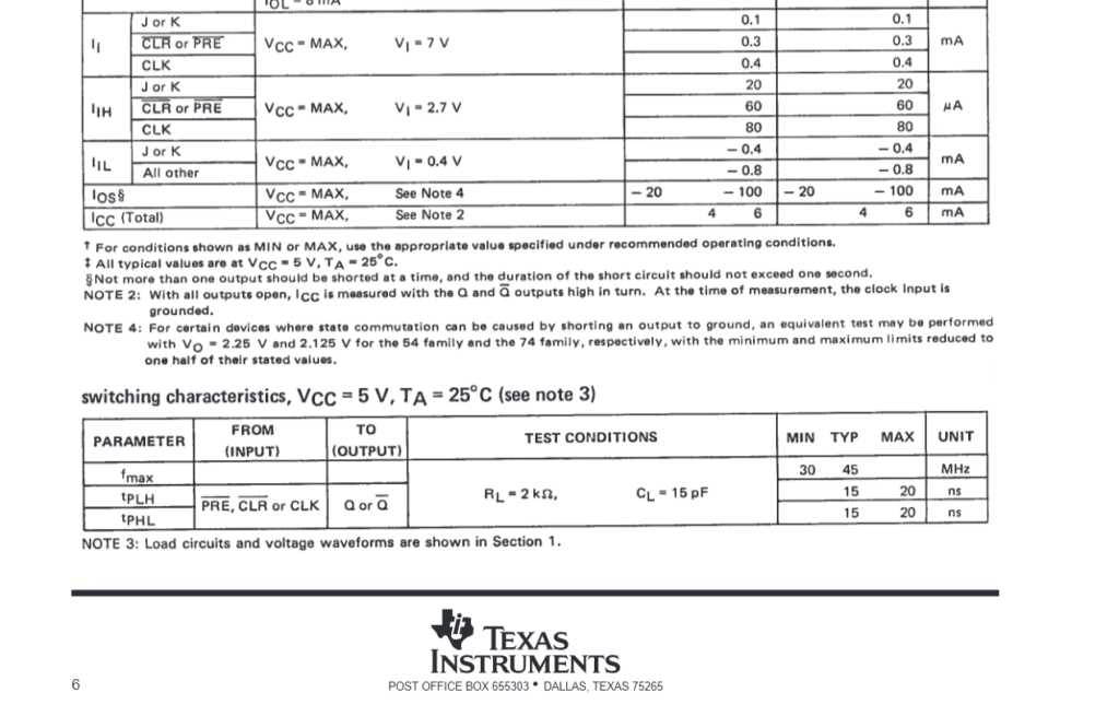
According to the SN74LS76A datasheet, the propagation delay is typically 15ns, and the input setup time, prior to the clock falling edge, is a minimum of 20ns.
So, from this, I surmised that an input level change, at the input of either flip-flop, should only clock through that single flip-flop on the next Clock falling edge.
So, next I did what I should’ve done in the first place.
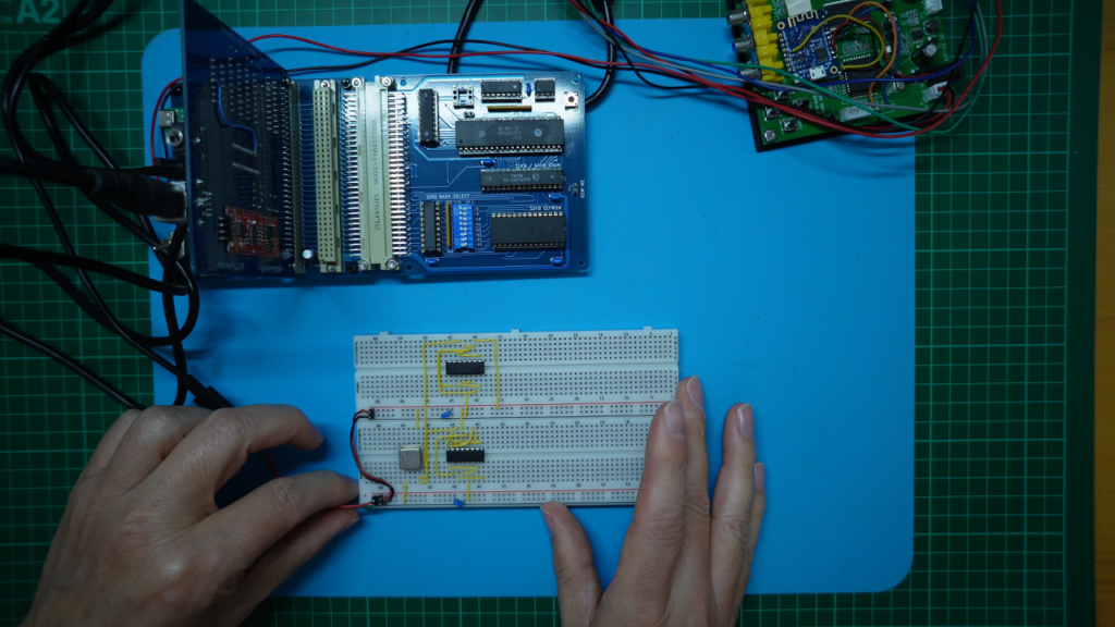
I put together the intended circuit on a breadboard, so that I could observe and verify its operation.
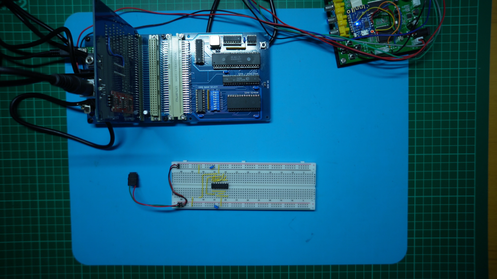
Having replicated the Quadrature clock circuit on a breadboard, I confirmed it continued to function unexpectedly.
So, my current theory is that the 74LS76A is allowing a high to low transition at an input, to be simultaneously clocked through both the sequentially connected flip-flops, even though the required minimum data setup time for the second flip-flop’s input could not have been met.
Next, I took a look at what other J-K flip-flops I had available in my parts drawers.
Since we don’t actually need the Preset input function, I found that I had some 74HCT73 dual J-K flip-flops.
These have the benefit of being a currently manufactured part, they have a higher drive capability, and are also only 14 pin (instead of 16 pin), as they don’t provide the Preset function (which we don’t need anyway).
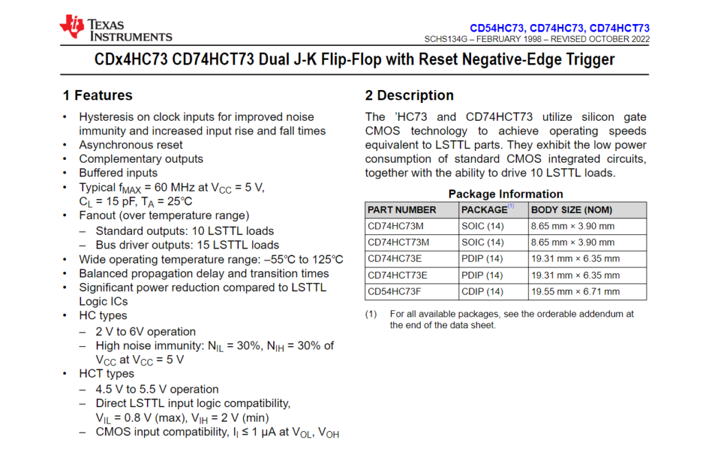
Otherwise, the 74HCT73 appears of similar function to the 74LS76A, being also negative-edge triggered. But hopefully the 74HCT73 behaviour, in particular with regard to the specified minimum input setup time, adheres to expectations.
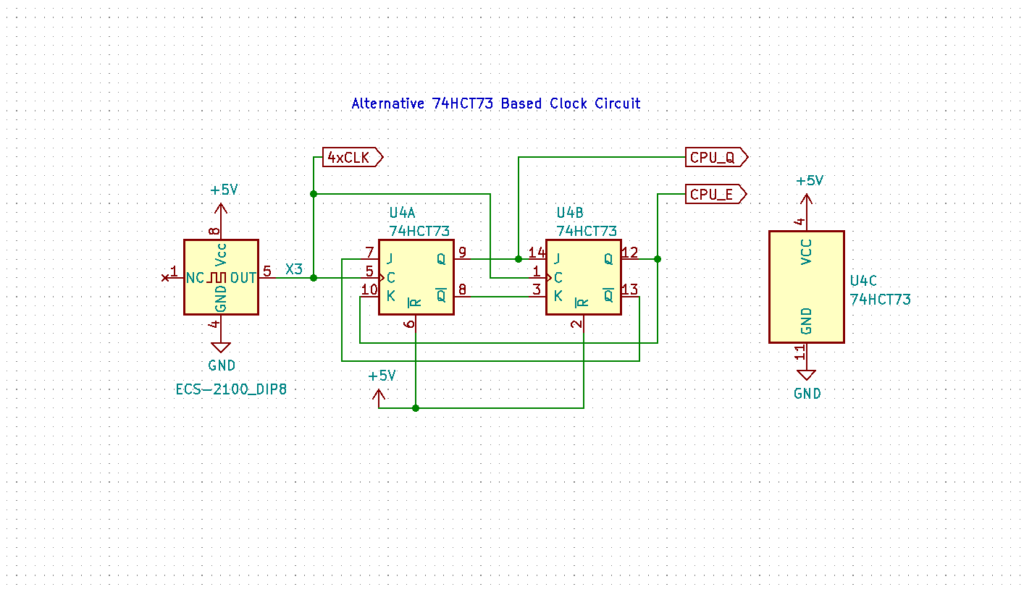
So next I tried out, on the breadboard, a similar quadrature clock circuit, but based on the readily available 74HCT73 chip.
Here is the schematic I’ve drawn-up based on the 74HCT73. It is basically identical to the original 74LS76 circuit, with the exclusion of the Preset inputs, and of course in a 14 pin pinout.
Here is my breadboard again, but with the addition of the 74HCT73 circuit.
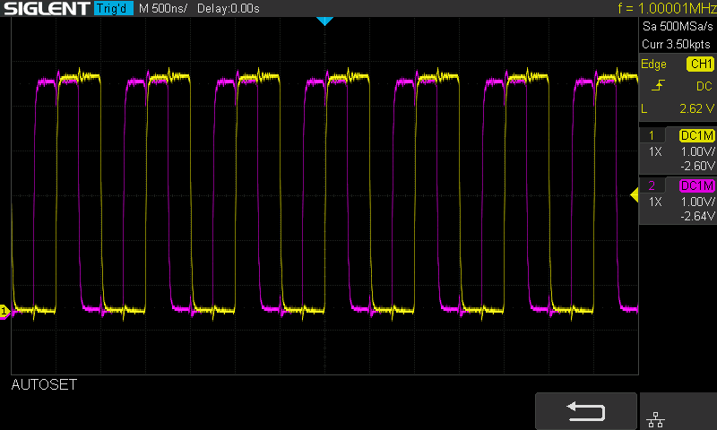
Having applied power once again, and viewed what we then got on the scope, we were now looking good!
We now have the expected 1Mhz 50% duty cycle quadrature clock.
This is great news!
I’m still not sure why the 74LS76A based clock exhibited that strange behaviour, but I’m certainly happier to instead use the 14 pin, still in production, 74HCT73, as an updated 6809E external clock generator.
So the last thing I did for today’s post was to patch across the replacement clock generator to our new v2 CPU card, so that I could test if the card is now fully operational.
All that was required was to wire 5 pins of the CPU Card’s 74LS76 socket, to bring power and the master clock signal across to the breadboard, and then to return the 74HCT73 generated Q & E clock outputs.
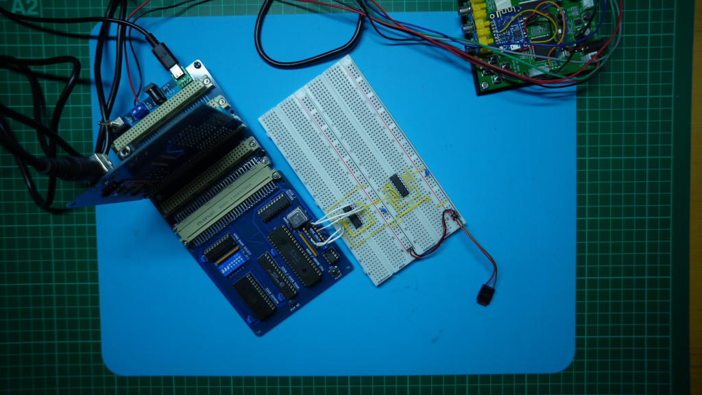
With that done we were able to once again try our external clock CPU test.
I turned on the power and… Finally we have our working video display test output.
So, we can close with some SUCCESS!
The next step for me is to update my “v2” CPU Card design to instead utilise the 74HCT73 chip for the External quadrature clock generation.
Along with an earlier missing Reset pull-up resistor connection oversight, the final 6809 CPU Card will then be at board revision v2.2.
Once testing of a new PCB is complete, I would expect v2.2 to be the final internal or external clock version of my 6809 CPU card!
Then, being finally happy with my 6809 CPU card design, I’ll next move on to my first I/O Card for the Minimalist Europe Card Bus.
I intend this to be a Motorola based I/O Card, to faithfully team up with my 6809 CPU Card.
This will then finally deliver my modular PCB based update, of my original 80’s Wire-wrap Eurocard 6809 system. But now with:
- A full 64KB populated memory space.
- I/O function separated from the CPU card.
- And, address-map configuration flexibility.
But, until then…