
This post follows on from my earlier Minimalist Europe Card Bus posts and videos.
The 6809 CPU Card has been a long journey. First v1.0 then v2.0, and now v2.2 will finally (hopefully), deliver on my desire to support either Internal or External clock variants of either the Motorola 6809 or the Hitachi 6309 CPU’s.
Join me as I walk through the schematic and PCB changes made for v2.2, and then assemble and test my first card.
You may recall that in my previous 6809 CPU Card post / video, I discovered a flaw with the originally intended external clock generator circuit.
Therefore, in that post we designed a replacement clock generator circuit and verified its operation on a breadboard, and finally completed verification of the original prototype PCB, by linking across the replacement clock generator to the original PCB.
Since then, I’ve updated the CPU Card schematic and PCB layout to a (hopefully) final version 2.2, and ordered the updated prototype PCB’s.
The new PCB’s have since arrived, so in this update I’ll go through the changes to the schematic and PCB layout, and then build and test the first v2.2 6809 CPU Card PCB.
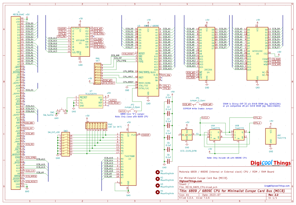
Let’s start by reviewing the Schematic changes.
Here’s the full v2.2 6809 CPU Card schematic.
Now, let’s zoom into the clock generator area of the schematic.
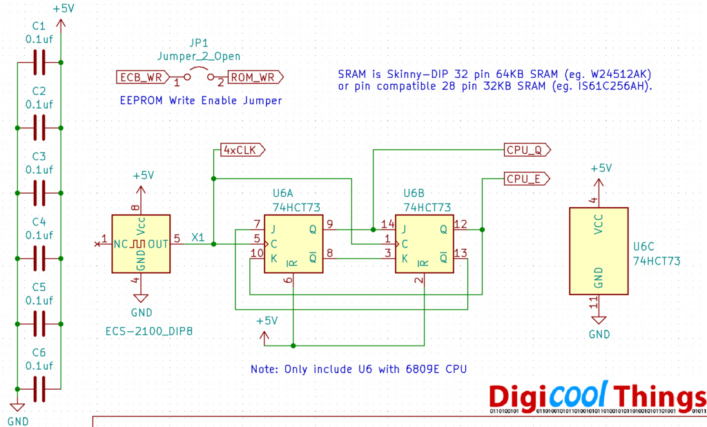
So firstly, the Clock Generator circuit has been updated to now use the 74HCT73 J-K Flip-Flop.
As the 74HCT73 comes in a 14 pin package (instead of 16 pins for the old flip-flop), it gives us a little more PCB space. So I also took the opportunity to add another 100nf bypass capacitor, which will be dedicated to smoothing the power routing for the Clock circuit.
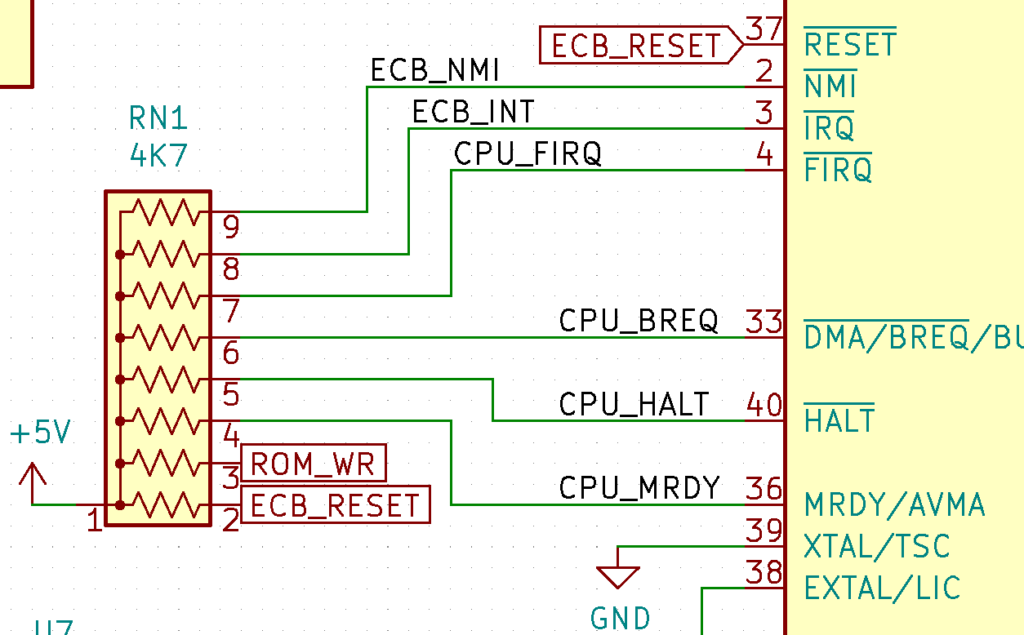
And finally, I’ve updated the schematic to specify a 4.7K Resistor Bank for the CPU pull-ups, instead of the previous 10K Resistor Bank. This was prompted by some test results in my previous post here, covering Retro CPU Interrupts.
Now let’s take a look at the PCB layout changes.
Here’s the full v2.2 6809 CPU Card PCB Layout.
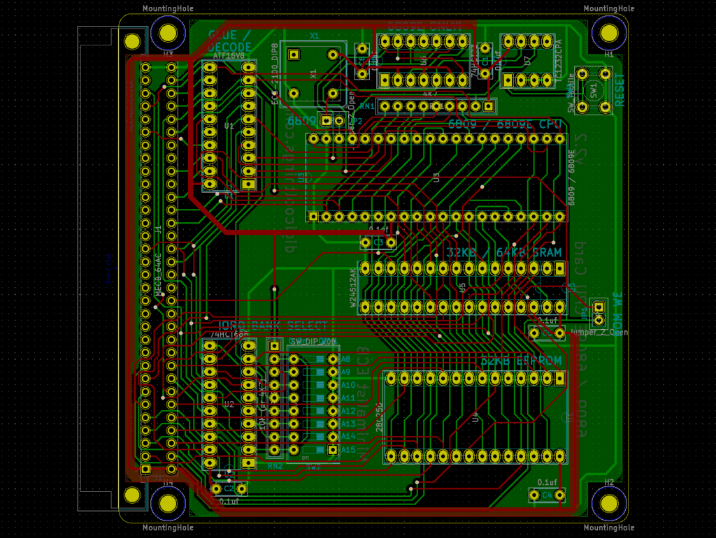
Now, let’s zoom into the clock generator area of the PCB.
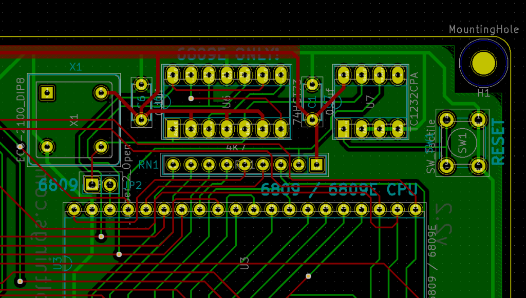
For the Clock circuitry I’ve moved the crystal oscillator over a little, to make room for the new bypass capacitor between the oscillator and the new 14 pin 74HCT73 flip-flop.
The power feed is then routed to this capacitor, and then on to the oscillator and flip-flop, providing additional smoothing of the switching noise from the clock signal.
In addition I’ve moved the “6809E Only” silkscreen message, to now sit outside the flip-flop’s IC socket, so it remains readable when the 74HCT73 chip is inserted.
And, that’s basically it for the v2.2 PCB.
Let’s take a look at the manufactured prototype PCB.
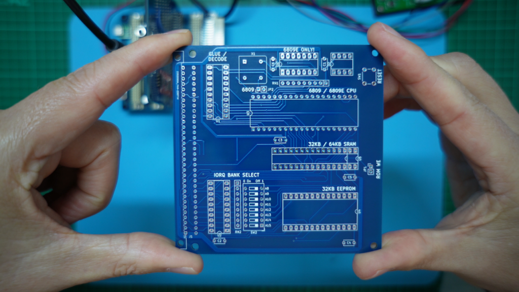
I think it looks great. So, let’s get one assembled.
For assembly, I started off with the bypass capacitors, and the two Single In-Line resistor packs.
Noting that the resistor pack next to the CPU is 4.7K. The other resistor pack can be either 10K or 4.7K. I’ve used 10K.
Then I soldered in the IC sockets, including the 8-pin IC socket that I’ve modified for the Crystal Oscillator, as explained in earlier videos.
I then also soldered in the 2 pin headers for the ROM Write Enable and the 6809 selection.
Then, the 8-way Dual In-Line switch and the momentary switch for the Reset.
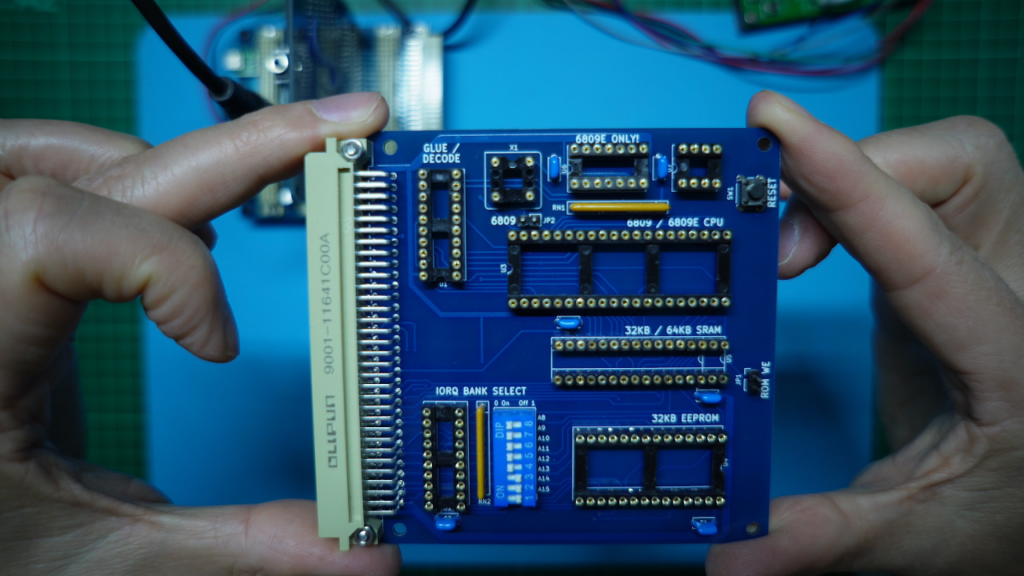
Finally, the male DIN 41612 MECB bus connector, which is secured in place with a couple of 10mm M2.5 bolts.
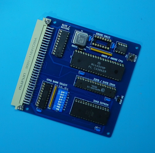
With the board assembly completed, it was time to get some IC’s inserted.
As we already had tested known good IC’s on the prior prototype 6809 CPU card, I just move these over.
Firstly, the 74HCT688 8-bit Comparator.
Then a 64KB Static Ram, and then our internally clocked 6809 CPU chip.
Also, the TC1232 8-pin reset chip.
Next, the 4Mhz crystal oscillator to run the CPU at 1Mhz.
As we did last time, I initially left the clock generator chip uninstalled, so we first test the Version 2.2 Card with an original internal clock 6809 CPU.
So, I also inserted the 6809 jumper, to feed the crystal oscillator clock directly to the internal clock 6809 CPU.
Finally, I also moved across the programmed PLD and ROM chips, which we had previously used for configuring and testing the earlier CPU card.
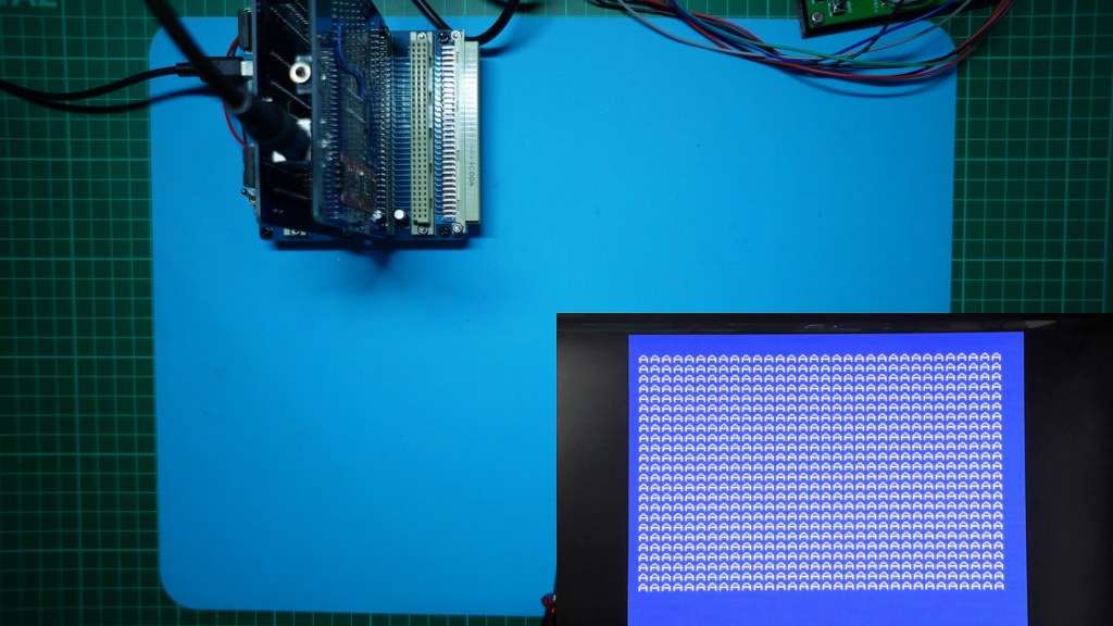
With the version 2.2 CPU card ready to go, we were now ready to insert it into our backplane, alongside the TMS9929 video card, for its first test.
And, with power applied, as expected we got the same successful video display test output.
So we have v2.2 CPU Card “Success” with using an internal clock 6809 chip, replicating the success of the earlier v2 and v1 prototypes.
Next, I tried the new CPU Card configured for the more common 6809E external clock CPU.
First I took out the internal clock CPU chip, and also removed the 6809 CPU jumper.
Then I inserted the new 74HCT73 J-K flip-flop chip, for the external quadrature clock generator.
Finally, I inserted the same Hitachi 6309E external clock CPU, which I’d early used when testing our v2 card.
With the card re-inserted in the backplane, and power re-applied, we were finally looking good.
With successful display test output again, we finally have complete “Success” with our v2.2 6809 or 6809E CPU Card.
As I mentioned at the start of this post, the MECB 6809 CPU Card has been a long journey.
First with a successful v1.0, which was based on my existing 80’s stock of internal clock 6809 CPU’s.
Then, the discovery that internal clock 6809 chips were now hard to find! With several ordered batches of internal 6809 and 6309 chips turning out to actually be 6809E variants, that had been incorrectly re-marked by the supplier as internal clock versions.
This then lead me to wanting to redesign the 6809 CPU Card to support either Internal or External clock variants.
The result was my v2 6809 CPU Card, which then unfortunately proved to be a failure, as the officially published External Clock circuit, that I had used, did not function as I’d expected.
This was also a good reminder / lesson, that this type of circuit function should first be verified, on breadboard, before proceeding to PCB layout!
Finally we now have a successfully tested, revised v2.2 6809 CPU Card, delivering on my desire to support either Internal or External clock variants of either the Motorola 6809 or the Hitachi 6309 CPU’s.
Now that I’m finally happy with our MECB 6809 CPU Card, we can focus on my first I/O Card. The design of which has now been completed, following on from my last two posts covering some of the design decisions.
At the time of writing, the first prototype I/O Card PCBs are on their way from JLCPCB.
When they arrive, I’ll be back to present my first Motorola based IO Card design.
Until then…
Soooo…… when can I grab some cards & build my own?
Hi Scott. It would be awesome having other enthusiasts also experimenting with my modular retro 8-bit system.
I had been holding off until I’d designed an initial set of cards, needed to make a more complete system.
I think, with this coming Monday’s post / video, I’ll finally be at that point, when I add my first I/O card with sound.
Perhaps I’ll add some listings to my Tindie store, with PCBs and options for some of the main components, to make it easier for others to assemble their own modular system?
Excellent! I’m interested in the modularity of this setup and intend to build a retro case to enclose it all in, though it doesn’t seem to be predisposed to fitting well into a retro case that would be reminiscent of circa 1970’s/1980’s 8 bit home computers… I guess I could have an amateur attempt at designing a backplane style pcb that might fit better, and point the interesting end of the cards (interfaces, ports, etc.) toward the rear, with a keyboard inbuilt into the case?
That’s just my pondering, but having something like this with a standardised bus that would be a dream to hack & modify, might be a far better option than trying to find my first computer to show my kids how I grew up, a Hitachi Peach, MB-6890 with its master basic level 3 – and your system being modular, future expansions like hardware sprites and fancy graphics and gaming with your upcoming joysticks and I/O cards might just quench the thirst.
Also, I have heaps of compact flash cards out of retired cisco equipment, which would be ideal to repurpose as drives along with the inevitable SD card interface you’d no doubt be looking to introduce?
I don’t really know as much as I’d like about electronics and computing, but I’m keen to project some things out though, and so far some land-boards tindie bought PCBs were fun to put together and get some Pi-Pico basic computers up and running – and now I’ve gone and bought ten HD68C09P/HD68C09EP cpus to play with, I’ll be tagging along… Also happy to see the selectable int/ext clocking option after hearing about your own woes with incorrectly advertised chips!
Yes, modularity was a key focus of the design, as I wanted to be able to add / exchange boards, to allow experiencing with the various 8-bit CPU’s, Video chips, and the general I/O chips I designed with back in the 70’s and 80’s.
As my design is built around economical 100mm square cards / boards, this makes for a “cube” shaped system when combined with the existing backplane. So, for a case, I had thought of perhaps eventually designing a 3D printed cube style case.
At this stage I’m just enjoying playing with some machine code on the 6809, which takes me back.
In the short term, my next CPU card plan is a 6502 card. Along with the flexible memory map design, my existing TMS992x Video card, and my new I/O card, I’m thinking I could then configure the system to imitate a CreatiVision and run some of the memorable early retro colour TV games I remember playing long ago. I always find it most nostalgic to run code on the real hardware of the day, avoiding emulation.
Aș regards learning more about electronics and 8-bit computing, I always say the best way to learn is hands on! There’s nothing like firing up your own retro system, and using the likes of a prototype card to start build and program new I/O interfaces etc.
An advantage of the early 8-bit CPU’s and Peripheral chips is that they are much simpler than modern devices, so it’s possible to get to know the hardware at the lowest level, which can assist with learning the fundamentals of computers and digital electronics, as a great basis for building a good technical understanding of how computing has since evolved.
Awesome! I envisioned using the same card/pcb dimensions, but instead of one backplane with 5 vertical and 1 right angle connectors, either have one backplane with two rows of three vertical connectors, allowing for the same expansion, but in a form factor that would suit a low profile appropriate for my envisioned case with inbuilt keyboard, or two PCBs with three vertical connectors each, connected by a flat ribbon cable, but again would easily accommodate a computer case similar to an Amiga/C64/etc. with integrated keyboard & power supply with three rows of interface expansion out the back – I can already see how I’d do it, and with heaps of cisco 1900 5v power supplies available in a pile here, an integrated power supply and fan would be the go. I can even imagine a case that might replicate a ribbon connected PCB forward below the keyboard that could make SD/CF/Joystick ports available from the front, just under the keyboard – but that’s a long way down the track. Looking forward to seeing it all come together, and when I do get some cards, I can play with designs and carve out some concept cases for fun – the idea of having a 6502/Z80 option cpu boards down the track, are a real attraction too, and now I’m especially interested… 😀 😀 😀
Yes, some thought would need to go into the best way to make a flatter / lower profile backplane, compatible with the keyboard case you are envisioning.
For now, my focus is just with the cube shaped open system look. Possibly, I’m just enjoying seeing the bare cards with their retro components, so a case is not an immediate priority for now.
But, I’d certainly be interested in hearing more about what you might come up with.
After designing a 6502 CPU card, I’m definately also intending on a Z80 based CPU card. I also spent a couple of years writing Z80 machine code back in the early 80’s, on a TRS-80 clone that I owned before moving on to the 6502 based C64. However, of these three 8-bit CPU’s, the 6809 remains my favourite 8-bit CPU to program.
I guess that would be another subtle request in future pcb designs, perhaps dupont header options for those of us who do want to build our projects into cases, and use remote switches/LEDs in them?
🙂
This is a good idea, that I’ll keep in mind. Thanks.
At the moment, things like the CPU reset switch would require soldering a lead to the existing switch pads to make a remote / case mounted switch. The only constraint I might have for doing this will be limited PCB space.
But having said that, my new I/O card (which will be shown in my next post / video), has IDC connectors & pin headers for all of the I/O ports. However, the sound output is still just a 3.5mm Audio connector mounted on the board.
Perhaps I should have included a header for sound output as well? Yes, good idea to keep in mind for future cards!
Awesome! You’re right – a header for a case speaker would be the go too, I’m sure I could solder my own in if I had to – Anyway, don’t rush it on my account, take your time and do it properly! I’m certainly in no rush myself…
You’ll be interested to know that you’ve prompted me to add a 2-pin header for Audio output to the new Motorola I/O + Sound card. Now, the v1.1 Schematic & PCB has headers for all possible connections.
I was already making a v1.1 update tweak, so added this extra header while I was doing that. 🙂
Note however, this is not a speaker output, as no amplifier is included onboard. The Audio output is just line-level, as it was intended for feeding into an external amplifier, or, linking across to the TMS992x Video card’s sound input to allow integrating with the Video card’s RGBS output connector (which can then feed the audio ouput signal, along with the video signal, to a monitor that supports audio).
Oh, and whether you’re considering a ps/2 or USB keyboard port, an internal header for those if space permits, would of course be an especially neat addition! 😀
I’ll keep this in mind also. But, I’ve no immediate plans for adding a ps/2 or USB keyboard port. Mainly as I’ve been focussed on re-living my late 70’s / early 80’s retro experience, when (of course) we weren’t using PS/2 or USB keyboards. But who knows, that might change as I progress.
Back in those days we were wiring up either Hexadecimal Keypads, or full QWERTY keyboards, that involved us having to wire-up all the keys with the necessary matrix wiring, and either writing the machine code for keyboard matrix scanning (via 8-bit I/O ports), or using a Keyboard encoder chip (for a parallel ASCII interface), that was also common at the time.
e.g. Like the National Semiconductor MM5740AAF, that I remember using when making parallel ASCII keyboards for connecting to our retro home-built computer systems of the time.