
As I mentioned in my earlier MECB posts, I wanted to be able to create MECB boards which implemented addressing flexibility.
This is to allow any I/O board design to be utilised with different retro 8-bit CPU boards, and with different memory maps. This would then support whatever 8-bit CPU based system design, I might want to explore & experiment with.
Another consideration is to (ideally), provide simplicity & consistency to the address decoding schematic, which could then be used as a template across different board designs. In addition, minimising the PCB board area required to implement the glue logic, whilst maintaining retro through-hole components.
When reviewing my old-school designs, from the early 80’s, there was typically a small handful of 14 pin and 16 pin TTL packages featuring in each address map specific Address Decoding Glue Logic design.
The logical conclusion is to utilise a retro PLD device, which (fortunately), Microchip (ATMEL) still produce as the ATF16V8, ATF22V10 etc.
Some folk may disagree with this approach, but I believe this is the logical solution for creating a flexible, but still retro, Address Decoding design. I would note the following points:
- Address Decoding is about the simplest and most basic use for which you can use a PLD device.
- Designing your Address Decoding logic is as simple as writing an Address Decoding logic statement.
- Programming an ATF PLD chip is really just as simple as programming an EPROM or an EEPROM.
- Many makers, who are into retro microprocessors, will no doubt already have a TL866 Programmer in their toolkit (for burning EPROM’s etc).
Design
The economical 20 pin DIP packaged ATF16V8 appears to have all that we need. In its Simple Mode, this device has 18 pins available, 8 of which are I/O and 10 are inputs only. In Simple Mode, 2 of the I/O pins are permanently configured as outputs only (pins 15 and 16).

As the ECB Bus utilises the MREQ & IOREQ approach of the Z80 (i.e. an allocated I/O address space), my thinking was that I’d utilise 15 pins of the ATF16V8 for inputs, allowing up to 3 pins to be used as Chip Select outputs. The 15 inputs are divided into:
- The 5 most significant 64KB address lines (i.e. A15 – A11), allowing for memory decoding with 2KB resolution.
- The 5 most significant I/O address lines (i.e. A7 – A3), allowing for I/O decoding with 8 byte resolution.
- And finally, 5 control lines (MREQ, IOREQ, RD, WR, and CLK).
Where this still isn’t sufficient for the required decoding, then an individual card design could (of course), still implement some supplemental gates to complete the glue logic, whilst still maintaining a minimal chip count and still retaining some PLD based Address Map flexibility.
Alternatively, some control lines could be swapped out. For example, if RD and WR were not required in the Address Decoding logic, for a particular board design, but perhaps M1 (on a Z80 system) might be desired etc.
By defining this initial ATF16V8 MECB standard pin allocation assignment, this enables a PLD to be included in my MECB standard board design KiCAD template, simplifying the process of designing a new board.
If sufficient PCB space is available, it’s also worth ensuring that the PCB space allocated for the ATF16V8 can optionally support a 20-pin ZIF socket, to provide for ease of Address Decoding swap-outs. In this way, when using a I/O board to experiment with different system configurations, it’ll be easy to just swap out the PLD for different memory map requirements. Of course, if building a more permanent system you could just utilise a regular 20-pin IC socket.
PLD Pin Assignments
The following input pin assignments have been made. These have been based on the ECB bus pin order of the signals, for ease of PCB routing, and was confirmed & optimised by the actual routing of the PLD while designing the KiCAD template.
Five most significant I/O address lines (i.e. A7 – A3):
- Pin 1 = A3
- Pin 2 = A4
- Pin 3 = A5
- Pin 4 = A6
- Pin 19 = A7
Five most significant 64KB address lines (i.e. A15 – A11):
- Pin 18 = A11
- Pin 7 = A12
- Pin 12 = A13
- Pin 5 = A14
- Pin 13 = A15
Five control lines (MREQ, IOREQ, RD, WR, and CLK):
- Pin 9 = CLK
- Pin 8 = IORQ
- Pin 11 = MREQ
- Pin 6 = RD
- Pin 17 = WR
Leaving the following three pins available for Chip Select outputs (noting Pins 15 & 16 can only be outputs):
- Pin 14 = CS0
- Pin 15 = CS1
- Pin 16 = CS2
PLD Programming
With the pin assignments determined, the next step is programming the address decoding logic that we require.
To do this I use two tools.
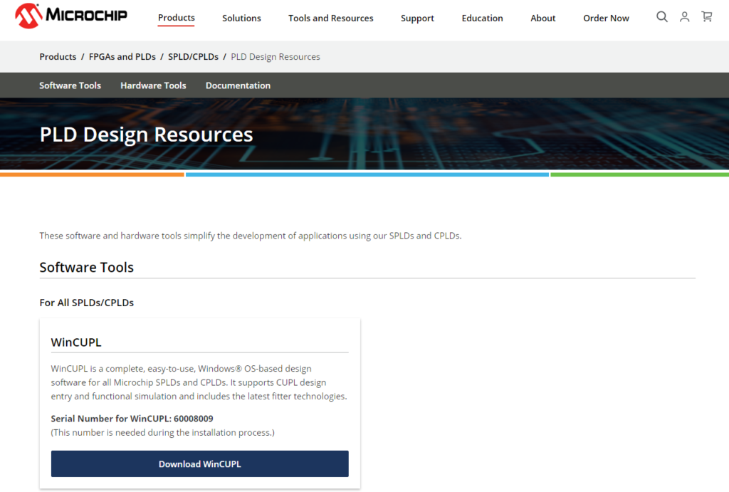
Firstly, the WinCUPL software, provided free by MicroChip, is used to design your logic and produce a JEDEC format file for programming into the PLD chip.
You should find a link to download your copy here: https://www.microchip.com/en-us/products/fpgas-and-plds/spld-cplds/pld-design-resources
You may also want to grab a PDF copy of the WinCUPL User’s Manual for a reference.

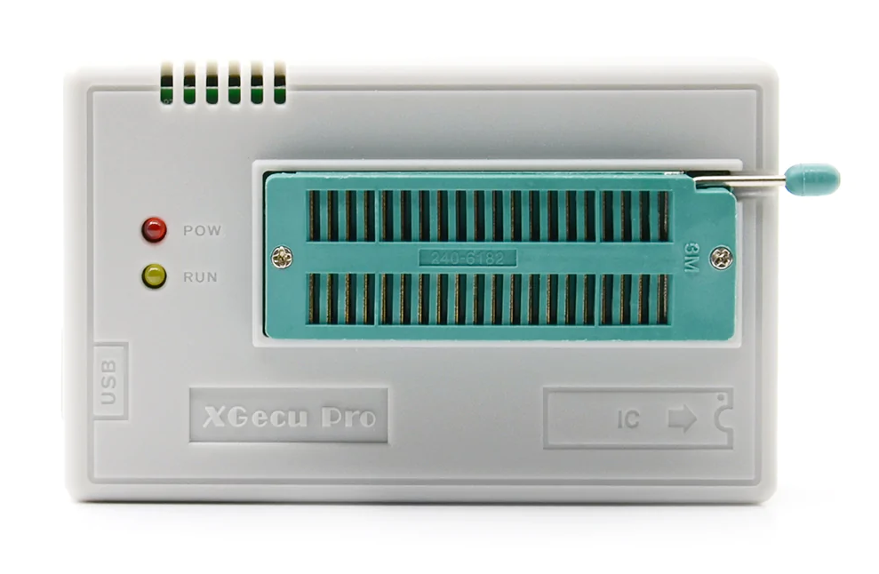
Secondly, I use the commonly available TL866II Plus EPROM Programmer to program the final JEDEC file into the PLD chip.
So let’s first take a look at WinCUPL.
WinCUPL
Once you have WinCUPL downloaded and installed, you should see a relatively blank window when you first start up the App.
As an example, I open my existing MECB_CHIPSELCT.PLD file to walk-through in the linked video.
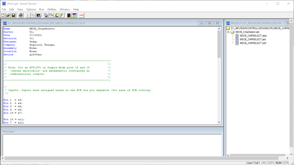
First you see that the .PLD source file has a header consisting of 9 reserved name fields. These are all the basic header fields, which I understand are all required to be present in the file. But only the Name field is required to have a real value in it. It is used to as the default compiled file output file name. So, it is logical to just insert the name of your source file here (without the extension).
The Device field allows you to set the default target device for compilation. You can set this manually via the Device Selection dialog box (Options -> Devices menu selection). But I’ve just set this Device header field to the appropriate Device Mnemonic for the ATF16V8 (B or C), which is g16v8a
Next, I’ve created a reminder source comment that for the ATF16V8, in simple mode, pins 15 & 16 are permanently configured as combinatorial outputs.
The actual code then begins, starting with the declaration of the input Pins, followed by the output Pins, which are filled in exactly as I described above (see: PLD Pin Assignments).
With the pins all allocated appropriate signal names, all that remains is to declare the logic equations that we want to apply for our Address Decoding logic requirements.
Easy.
In the linked video you’ll see that I created a couple of real world examples, to get started.
The first example is a Simple PLD Test, where we simply get our 3 configured output pins to follow 3 of the input pins.
I then created a simple breadboard circuit just to enable demonstration and verification that the whole WinCUPL -> TL866 Programmer -> ATF16V8 chip programming process, is successfully working as advertised!
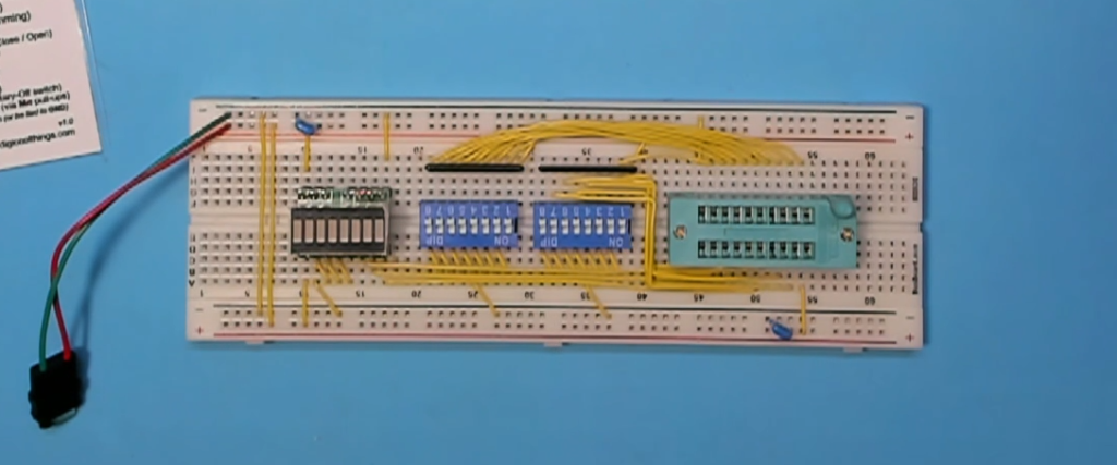
I demonstrate the successful verification of this simple PLD test on the breadboard in the linked video.
Again, back to WinCUPL, under the Option -> Complier menu option it’s important to check you have “JEDEC” selected under “Output Files”
Then we select Run -> Device Dependant Compile, or hit the F9 hotkey.
All going well, this should result in a dialog box indicating “Compilation successful!”, and also a .JED file in your project directory.
We can now program the compiled .JED file into a ATF16V8 PLD chip.
TL866II Plus Programming of PLD
Using the popular low cost TL866II Plus programmer, it’s as easy programming a PLD chip as it is programming an EPROM.
Simply select the appropriate PLD device (e.g. the ATF16V8 device for our purposes), then load your .JED file.
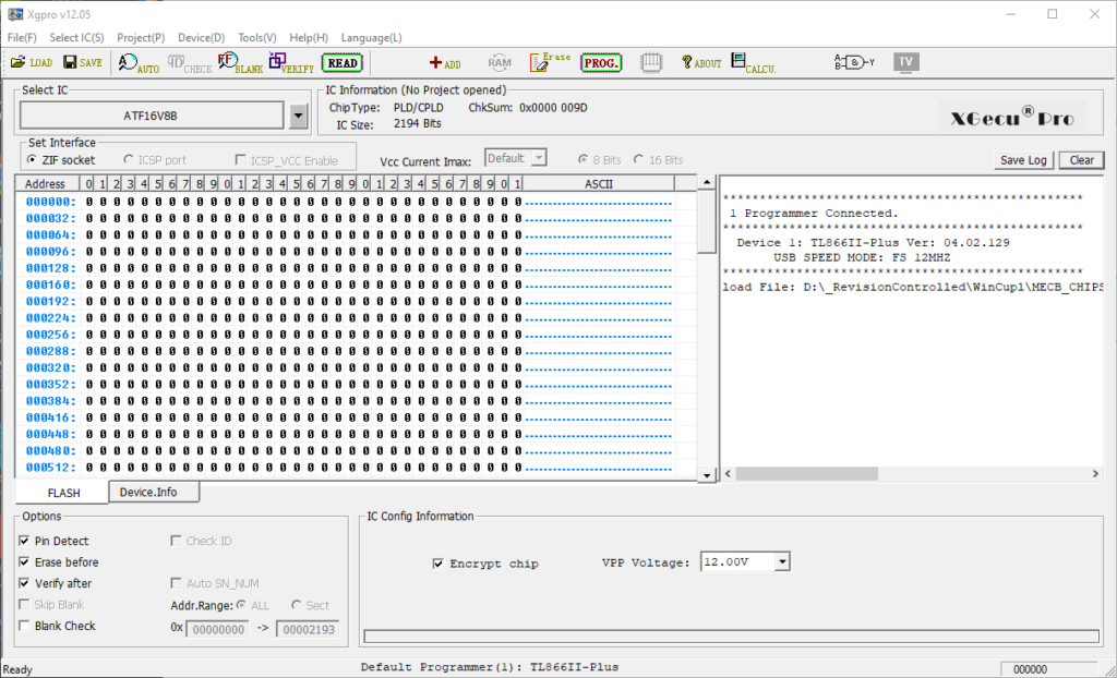
You’re then ready to program. There’s also an “Encrypt chip” checkbox, which you’ll want to ensure is unchecked if you want to be able to read back the chip contents at a later date. With the check-box ticked you will also disable the ability to successfully verify the chip later (until the chip is again erased).
CreatiVision VDP Address Decode Example
After proving the simple PLD test is successful, I created a second test example based on the decoding logic for the VDP chip in the CreatiVision.
The CreatiVision was an early 1980’s TV Game and Computer console. It was based around the 6502 CPU and the TMS9929 VDP (for the PAL version).
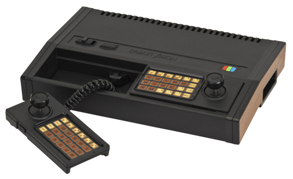
In the CreatiVision, the TMS VDP is memory mapped to use the 0x2000 – 0x3FFF memory space. Yes, even though the VDP only needs two address locations, it was allocated a whole 8K of the address space. This wasn’t particularly unusual at the time, as it simplified the address decoding gate logic that was required.
A VDP Read (CSR signal) is decoded for the 0x2xxx address block, and a VDP Write (CSW signal) is decoded for the 0x3xxx address block.
Of interest, is that the simple CreatiVision VDP address decoding circuit doesn’t gate in the 6502’s Read / Write signal. This therefore relied on the system programmer ensuring they didn’t issue a write command to the 0x2xxx address block. As this would therefore cause a bus driver conflict, with both the CPU and VDP data bus drivers simultaneously attempting to put data on the bus. This has the potential of overloading and damaging the drivers of either the CPU or the VDP chip.
We, of course, now have the flexibility of the PLD to fix this potential conflict, by including the Read (RD) and Write (WR) signals in the PLD based address decoding logic.
However, for the video demonstration, I just emulated the original CreatiVision address decoding logic.
Conclusion
The CreatiVision VDP address decode logic was also demonstrated as successfully programmed into the ATF16V8 chip, leaving us now ready to progress to creating our first functional MECB card.
Perhaps a VDP card? But, until next time…
Still coming to grips with how logic decides it’s using memory or decoding I/O of some device/card on the bus – I think I understand it to be the memory logic ignores the dedicated I/O space, and other cards using that I/O space in their logic, would take the role of that addressable memory allocation (for want of a better description), right?
You’re fundamentally correct.
To explain further, processors like the Z80 include a seperate 256 byte I/O address space and directly output IORQ (I/O Request) and MREQ (Memory Request) control signals, to indicate which address space is being addressed.
The 68xx and 6502 processor families just have a single 64K address space and you therefore just map I/O devices to any memory address block.
When implementing a Bus that is also compatible with a dual address space processor (like the Z80), it is common to have 68xx & 6502 CPU Cards emulate the dual address space by pre-allocating 256 bytes of the Memory space to be used exclusively by I/O devices, and generating Z80 equivalent IORQ & MREQ signals, to identify this.
Basically, IORQ & MREQ are never activated simultaneously, with IORQ stealing a selected 256 byte page from the single 64K address space on a 68xx, 6502 etc.
For MECB you can see this Bus Control Logic in the current MECB_CHIPSELECT_6809_CPU.PLD source file on the GitHub MECB repository.
Hope this helps clarify this.
Excellent!! Thanks Heaps for that! I feel less afflicted with stupid now, though only marginally.
Another question, amongst the downloadables on github, I can’t find any other KiCAD projects besides the template MECB – is that right? i.e. no KiCAD model for the backplane I could use to cheat with?
😐
Yes, for the moment I’ve published the PCB gerber files for the projects completed to-date, so that anyone can get their own MECB PCB’s made, if that is their preference instead of ordering via my Tindie store.
The KiCAD template helps give a headstart for anyone wanting to design their own new MECB card in KiCAD.
I’ll email you directly regarding the backplane KiCAD project, to see if I can help you out with that.