
Introducing the Motorola MC6802 CPU Card, designed for the MECB bus.
This takes me back to the original MC6800 days of the late 1970’s, and also rounds-out my collection of Motorola based CPU Cards, for my MECB platform.
Join me, as I walk through the project background, design, assembly, development of monitor firmware, and the example use, of this original 8-bit MECB CPU Card.
Background
This new CPU Card returns me to my first hands-on microprocessor days.
Having already created two flavours of Motorola 6809 CPU Cards (both, DIP packaged and PLCC packaged, CPU Cards), I’ll also mention that the 6809 remains my all-time favourite 8-bit CPU.
Then, after recently adding a 68008 CPU Card, I think it’s now time to round-out my Motorola CPU collection, with an original 6800 based CPU Card.
As noted, the Motorola 6800 CPU was the first microprocessor which I personally experienced, back in the late 1970’s.
This was in the form of the DREAM 6800. Which was also the subject of my latest re-creation project, which I recently featured in my 2025 RetroChallenge competition entry.
MC6875 Dual-Phase Clock Generator History
One of the challenges of putting together the original DREAM 6800, back in 1979, was (at that time), the global shortage of MC6875 dual-phase clock generator chips.
The MC6800 microprocessor itself was first shipped in 1974, along with a relatively expensive hybrid clock generator module, the MC6870 / 71 series.
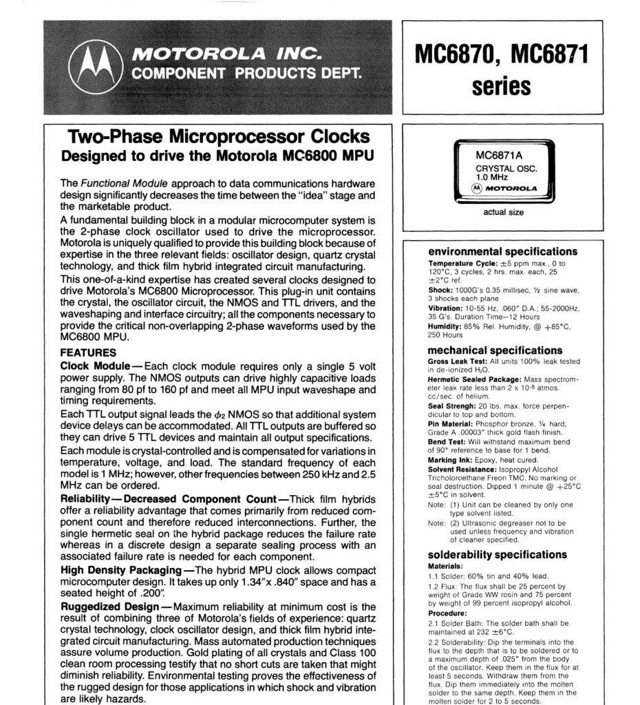
Later, in 1977, Motorola released the MC6875 clock generator, as a lower cost DIP16 packaged IC.
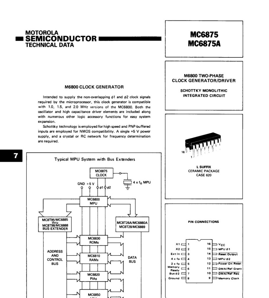
The MC6875 subsequently became the preferred, and standardised, dual-phase clock solution for the MC6800 microprocessor. This, no-doubt, contributed to it’s shortage at the time of the DREAM 6800 release a couple of years later.
At the time, a couple of solutions were offered for the enthusiasts wanting to build their own DREAM 6800 project.
Firstly, a circuit designed by Michael Bauer was published by Electronics Australia, as a substitute for the hard to find MC6875.
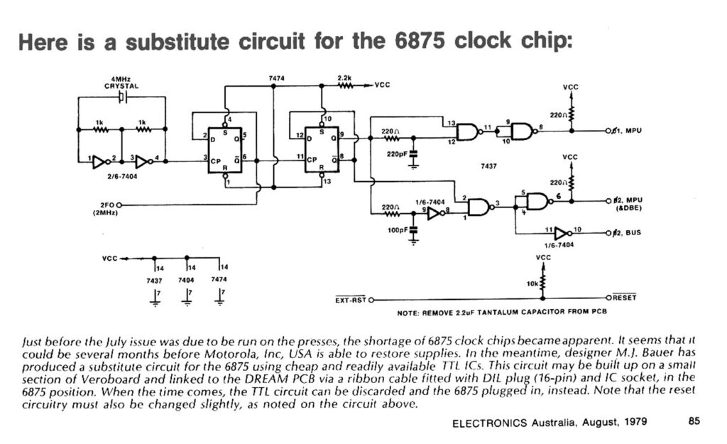
Secondly, a revised version of the DREAM 6800 was made available from kitset providers, which instead used the newer 6802 microprocessor chip instead.
MC6802 & MC6808 Release
In the same year as the MC6875 clock generator chip was released, 1977, the MC6802 was also released.
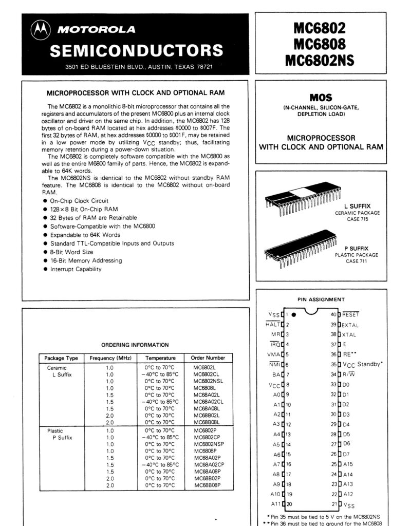
These days, I found that the MC6875 is perhaps even more difficult to source.
Fortunately, the 6802 took the original 6800 CPU, and simplified systems design, by including the dual-phase clock generator, on-chip.
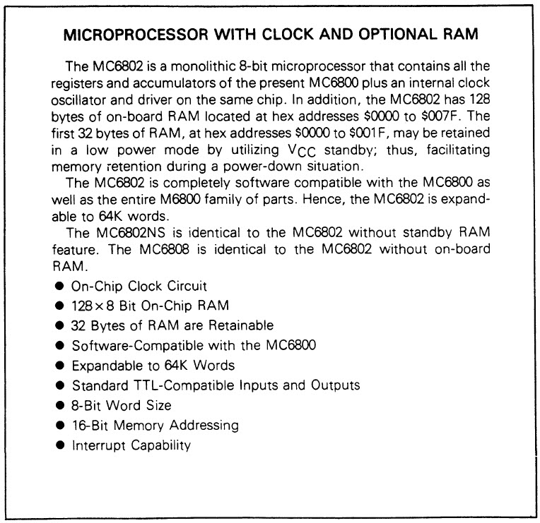
The 6802 also included 128 bytes of RAM memory on-chip. A separate standby-power pin was also provided, which allowed the first 32 bytes of the 128 bytes of RAM to be retained when the main power was removed.
This meant that, at the time, the MC6802 was also ideal for building small dedicated microprocessor based solutions. It no longer needed an external clock generator or external RAM (for making a small system).
With a 6802 you could build a powerful and flexible microprocessor based controller solution, with just a 6802, ROM, and perhaps a 6821 PIA for the I/O.
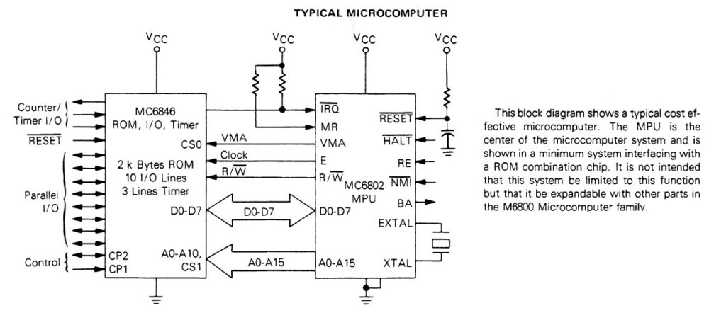
In fact, by using the MC6846 ROM, I/O, Timer chip (or RIOT as it was commonly known), you could build a 2 chip microcomputer system.
The 6802 also provides an input pin to allow disabling the on-chip RAM.
This allows the 6802 to effectively be used as simply a MC6800, with an in-built dual-phase clock generator. So, no longer needing a MC6875.
In addition to the MC6802, there was also a MC6808 released. The 6808 is essentially a 6802 without the on-chip RAM.
The only real-world incompatibility between the 6802 and the original 6800, is in terms of tri-state output drivers, to simplify its use in a Direct Memory Access (DMA) based system design.
Interestingly, the DREAM 6800 system used DMA for the Video interface.
Effectively, the original DREAM 6800 would halt the 6800 processor, during the active display area, in order for the display interface to directly access the display buffer memory locations, via the bus.
The 6802 based DREAM 6802 therefore had to implement a modification to avoid bus contention.
As I recall, this was achieved with the cheap solution of including resistors on the bus interface, to avoid destructive bus contention.
Not an ideal solution, but workable in an application specific, lower frequency, system design.
For our purposes, of experimenting with the 6800 processor on our MECB system, not having DMA functionality available is not really a concern.
Even my recent 6809 based DREAM 6800 recreation did not use DMA, as we now have better solutions for display generation, that don’t involve halting the CPU!
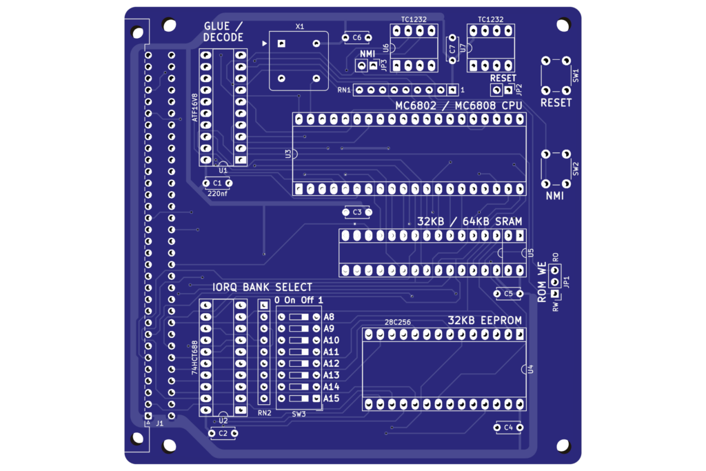
6802 CPU Card Schematic
So, let’s take a look at the new 6802 or 6808 based CPU Card schematic.
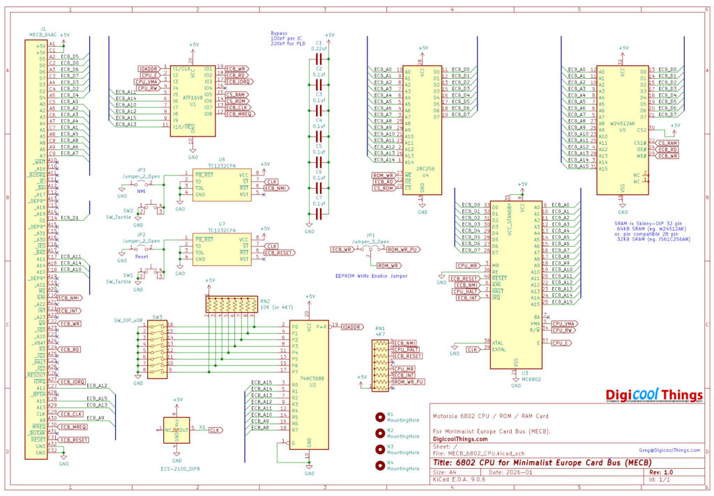
Firstly, as with most of the MECB Cards I’ve designed to date, the memory map defining glue-logic is implemented in a standardised ATF16V8 Programmable Logic Device (PLD).
For more detail on this choice and how it has been implemented, be sure to watch my earlier video “Address Decode / Glue Logic ATF16V8“.
Next, you’ll see that I have implemented two TC1232 DIP8 packaged Microprocessor Monitors, for the power-up and manual Reset control, and also for a manual Non-Maskable Interrupt (NMI) control.
Besides the power-on Reset, this provides clean, switch debounced, manual push-button control, for both system Reset and for a Non-Maskable Interrupt. All with no external components needed, but still in retro friendly Dual-In-Line Through Hole packages.
For more details on this reset design choice, you can watch my earlier video “Optimising our Retro CPU Reset Design“.
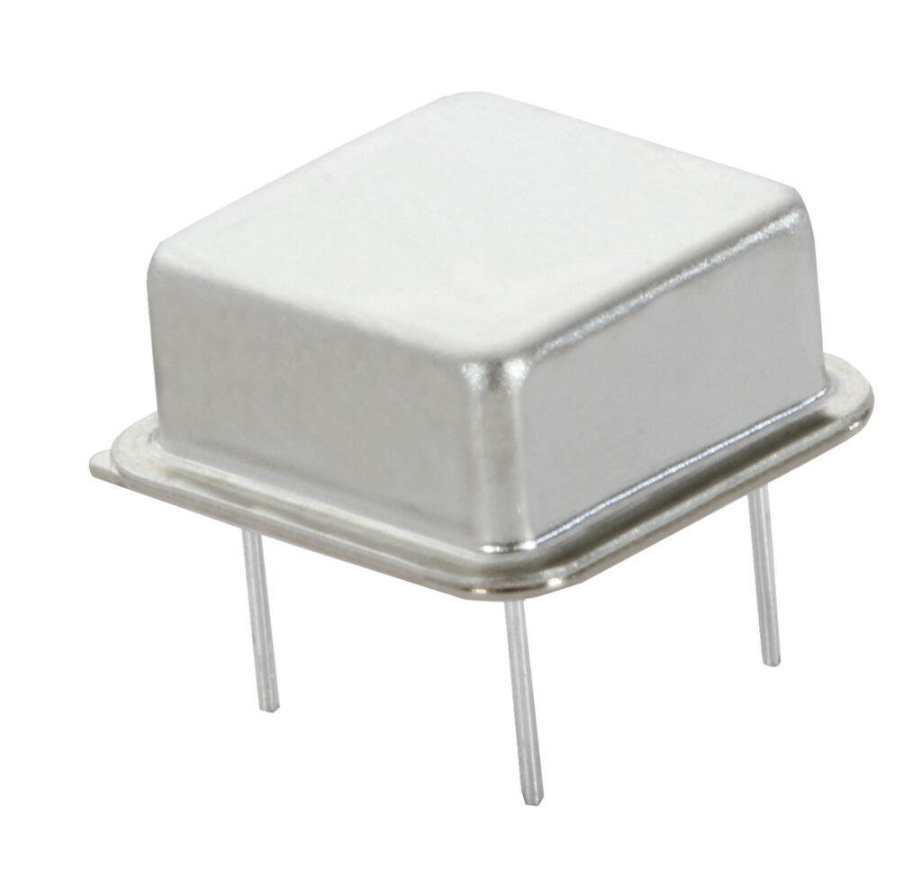
Next, we have a simple half-size DIP8 package Crystal Oscillator for the system clock.
In the old days we would typically use a parallel resonant (or parallel cut) crystal, together with a couple of load capacitors, to enable the on-chip oscillator via on-board clock generator XTAL and EXTAL pins.
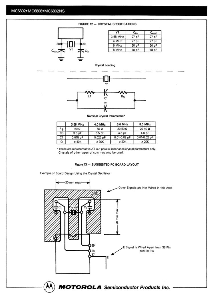
This also required careful PCB layout and careful selection of load capacitor values, in order to achieve an accurate and reliable Crystal clock source.
These days, complete crystal oscillators, in convenient DIP8 sized packages, are cheap and are definitely the way to go. They also need no external components, so there’s also no need for selected load capacitors.
Next we have my familiar 74HCT688 based I/O Request address space selection logic.
This enables you to select any 256 byte bank from within the 64K address space, as being reserved for the I/O space.
This emulates the separate Z80 I/O address space, by borrowing a 256 byte block from the 64K memory address space of other processor families (that don’t use a separate I/O address space).
An 8-way DIP switch allows full flexibility in dictating where this 256 byte space is borrowed from.
By doing this we can comply with the ECB bus standard of providing separate memory request and I/O request spaces, ensuring the bus can be compatible with both the Z80 and other 8-bit processor families.
Next, to avoid the need for individual pull-up resistors, we use space saving Single In-Line (SIL) resistor banks (or resistor networks), RN1 and RN2.
This all makes for a very tidy CPU Card, where the only individual discrete components, are the necessary bypass capacitors, located close to each Integrated Circuit power pin.
Here you can see we have six 100nf (0.1µf) bypass capacitors, for the six individual ICs, with the exception of the ATF16V8 PLD.
For the PLD we use a 220nf bypass capacitor. This is the value which Microchip recommends for their PLD devices.
Next we have a single chip 32KB EEPROM chip (28C256), for holding our ROM code, and we also provide for a single chip 64KB Static RAM chip. This enables us the full flexibility of allocating up to 64KB of our address space to RAM, and up to 32KB of our address space to ROM.
In combination with the PLD based glue logic, this gives us almost complete flexibility in our address map configuration, without needing any circuit changes!
Perfect for the 8-bit experimentation intent of our MECB platform.
It’s also something we would have died for back in the early days, when memory was expensive, and significantly smaller.
My first experience with building microprocessor systems, was with 2114 DIP18 packaged RAM chips, of which you needed 2 chips just for 1KB of RAM.
But, at the time this was actually awesome, as previously we had needed 8x 2102 chips to make up 1KB of RAM. Each chip being 1K by 1 bit (hence 8 chips to make up a byte).
Typically, when you made a new system, memory was the most expensive part, and expanding the memory beyond a few KB, would generally require a memory expansion board full of chips!
So, the fact you can now get a skinny DIP packaged single chip, that holds a full 64KB of really fast Static RAM, is really just incredibly awesome (for us nostalgic folk)!
Finally, we have the 6802 (or 6808) processor, which is the heart of the CPU Card!
The connections are pretty straight-forward, with the only real note being the RE (or RAM Enable) pin, which is grounded to disable the on-chip 128 bytes of RAM, effectively making the 6802 into a 6808.
Or, in other words, simply a 6800 processor with the addition of the on-chip dual-phase clock generator!
6802 CPU Card PCB
Okay, let’s move on to the 3D render of the routed PCB.
This PCB layout was based on updates and trace routing optimisations to my earlier 6502 CPU Card. So the overall layout is pretty mature!
Improvements, in the form of optimisation of routing and improvements to the silk-screen labelling and font sizes, and also the 220nf PLD bypass capacitor, will then be rolled-back into the existing 6502 CPU Card.
I know I’m biased, but I truly think it is a thing of beauty!
6802 CPU Card Assembly
So, it’s time to get the first one assembled.
My Online Store features a photo of the PCB and the Optional Packs, which are available to provide a complete Kitset for building your own 6802 CPU Card.
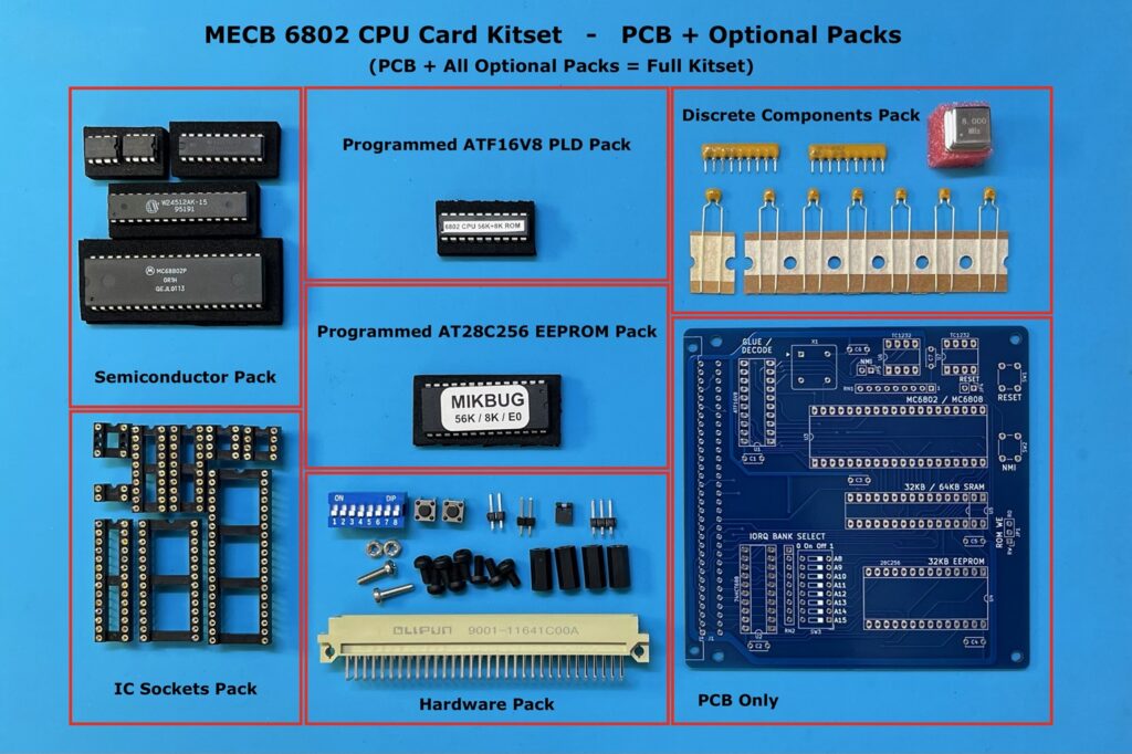
If you’d like to see a walk-through of the assembly steps, then be sure to watch the linked video. Chapters are also listed (in the video description), so you can just jump straight to the assembly section.
WinCUPL PLD Source Code
Below is the first page of the source code for the ATF16V8 PLD.
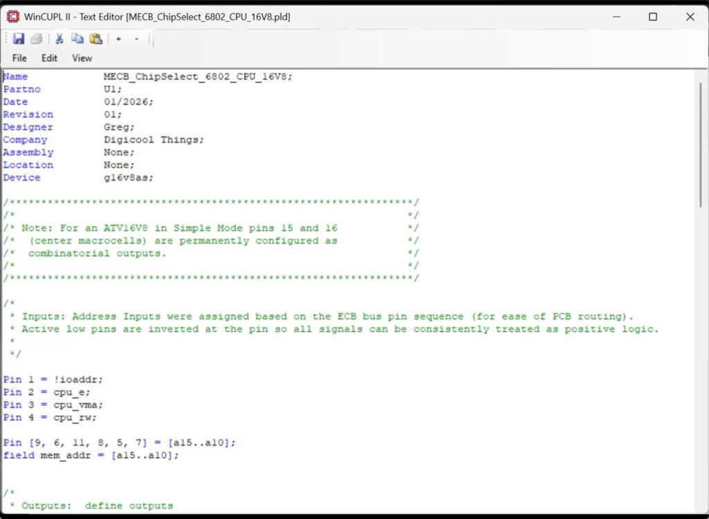
First we have the header, then we have our pin definitions.
As you can see, I invert the active low signals at the pin.
By doing this, all of the logic equations can be based on positive logic, for significantly easier to read logic equations.
So, first we have 4 control signal input pins defined.
These are, the active low I/O block selection, plus three bus control signals from the CPU.
Firstly, we have the CPU phase 2 clock output, also called Enable (E).
Then, we have the CPU Valid Memory Address (VMA) signal.
And, we have the CPU Read / Write signal (R/W).
Finally, to complete the PLD inputs, we have address lines A10 through A15, which allows us to define the on-board RAM and ROM memory map with a 1K resolution within the 64K address space.
I’ve also mapped the address lines to a “field”, which I’ve called mem_addr (or memory address), which allows us to use easy & very readable, memory address ranges.
Further down the source listing (which you can obtain from the MECB Github repository), you can see I have 8 pins defined for our outputs.
Note that this is a CPU card, therefore we are originating the MECB Bus Control signals, which you can see in the listing as the outputs prefixed “ecb_”.
Again, you’ll see that active low output signals are inverted at the pin, which allows us to treat everything internal to the PLD as positive logic. i.e. Active high logic.
So, in addition to the bus control signals, there are 2 Chip Select outputs for the onboard ROM and RAM, and also a spare Chip Select output. This is because our standard MECB use of the ATF16V8 PLD, defines 3 chip select output pins.
After we have defined our output pins, we then move on to our first logic equations.
These are to define our 5 bus control signals.
Here, we pass the CPU “E” clock signal directly to the bus clock.
The other 4 signals are conditioned with the CPU “Valid Memory Address” (VMA), to give us the bus Memory Request, I/O Request, and independent Read and Write signals.
In addition to the Valid Memory Address criteria, I’ve also conditioned the bus signals with the CPU “Enable” clock.
Although, this may not be necessary for some of our bus connected peripheral cards.
An example is the Motorola I/O Card. The Motorola peripheral family are all clocked directly with the CPU Enable signal (via the bus clock).
Also, individual peripheral cards can choose to include the bus clock in their own chip select logic.
However, since our memory chips are a lot faster, than they were in the early days, we really have no need to utilise an extended Valid Memory Address (VMA) period.
Even with the 2MHz clock, of the fastest MC68B02 CPU, this gives us a 250ns high period of the Enable clock. Plenty of time for our typical 150ns access time 28C256 EEPROMs. And our RAM is even faster.
So, I’ve chosen to pre-condition the bus control signals with the Enable (E) clock, simply on the basis that this should give maximum compatibility to other Cards with differing chip select logic.
But, you’re obviously free to play around with this, if you see the need.
Okay, next we move onto the onboard memory chip select logic.
Thanks to the memory address “field”, this is incredibly easy to read and setup.
First I have a block which defines, what I’ve called the default, of a 56K RAM and 8K ROM memory map, as I suspect this will be the most commonly used.
Having 56K of RAM in the early days would have been mind blowing. Likewise, having a full 8K of ROM space. In the late 1970’s we were lucky to have a few KB of RAM, and maybe 1 or 2KB of ROM.
So, this CPU Card enables exploring the original MC6800 CPU, with a fully loaded 64K memory space!
If you now refer to the last page of the source code, you will see that I have included (commented out), memory map alternates for 48K RAM / 16K ROM, and also 32K RAM / 32K ROM.
But you can also, easily enough, define any memory map with RAM and ROM space allocated anywhere, using 1KB boundary increments.
Okay that completes our PLD logic.
ROM Monitor Background
So, with the PLD logic explained, let’s move on to the ROM code.
Interestingly, when I started with this project I had fully intended on using just the original Motorola MIKBUG monitor program.
However, completing this video was a little delayed, due to the various other projects that I’m also working on.
So, when I had time to come back to this project, I’d already completed some more research (and some coding), and I had ended up cobbling together my own monitor version.
The monitor I ended up with was inspired by the various monitors which I had found available, for the MC6800.
MIKBUG was the original, popular monitor, released by Motorola for the 6800, back in the day, but it was also very simple.
Later, there was also Ed Smith’s SmithBug and various other variations that others had developed.
With more ROM space available to us these days, it made sense to be a little more extravagant, and include more functionality.
So, in addition to making more commands available, I’ve also implemented a useful Help screen, which is also highlighted, at power-up, by our initial cold start header.
It’s therefore self evident, and very easy, to remind yourself of the various commands that are supported, every time you power-up!
One of the frustrations of earlier monitor variations, was that standard monitor routines (which are called by user programs), were not more permanently standardised via a fixed address, monitor routines jump table.
This was mostly because, in the early days, ROM space was at a premium, and typically the available space didn’t allow for the luxury of a jump table.
So one thing that I’ve done, is to define a fixed address jump table to useful routines, located at the beginning of ROM. This means that the monitor can continue to evolve, without breaking compatibility with any user programs, which might have been written to make use of those routines.
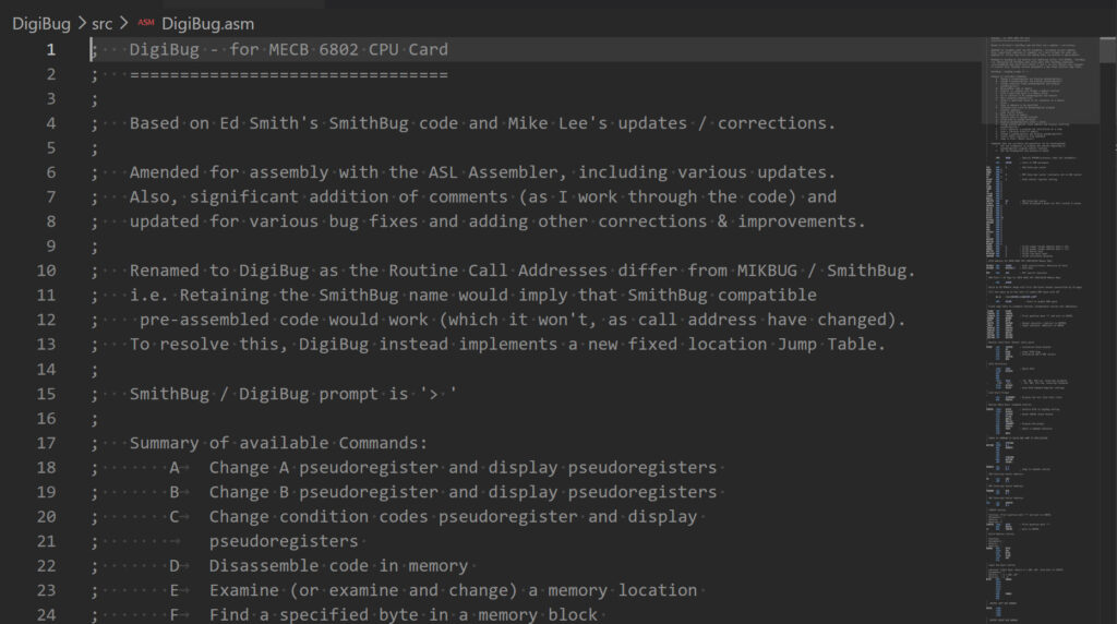
DigiBug Monitor User Routines
Below are the current routines, provided as a DigBug.inc include file, which can then be easily included in your own programs.
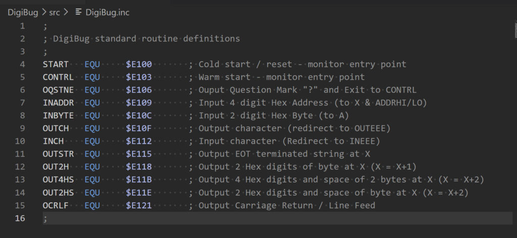
Due to this fixed address monitor routine jump table implementation, I’ve also chosen to call the monitor DigiBug.
This made more sense than calling it something like SmithBug V3 or V4, as that would have implied that any existing assembled code, which was written for MIKBUG of SmithBug, would just run without re-Assembly!
Despite differing memory maps, naming the new monitor DigiBug fully resolved this potential misunderstanding.
And, Yes, I can hear you. I did consider DigiMon, but that just wouldn’t have been right!
Now, because this monitor source code is quite lengthy, I’m not going to walk through it here.
It’s also a work in progress, as I continue to comment the code, to my usual standard.
But the commands are already functional enough to get us up & running with all that we really need.
So, the best way forward is to just demonstrate the monitor use, in practice.
Therefore, I move on to getting the programmed PLD, and my new DigiBug programmed ROM installed.
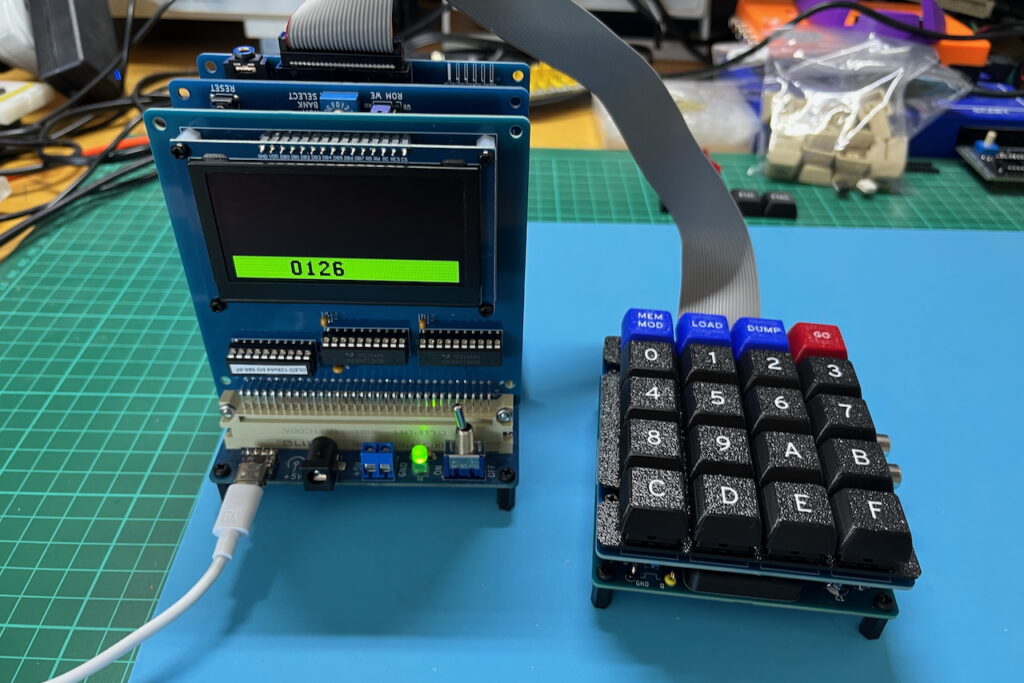
Now to test the new CPU Card out, I’ve just got my regular MECB backplane, and a MECB Motorola I/O Card for providing my serial UART connection.
Initial Power-up & DigiBug Use Introduction
After inserting the cards in my MECB Backplane, I apply power.
And we’re up and running. First, you can see the cold start header, which notes that “H” will give you help.
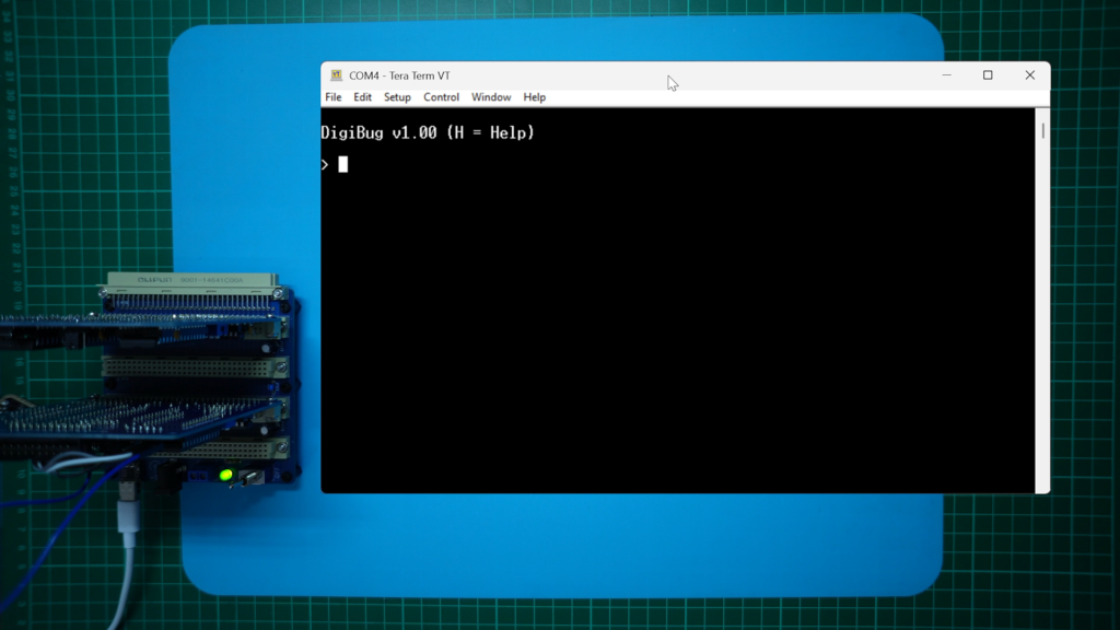
If you’d like to see a walk-through of some initial DigiBug command usage, then be sure to watch the linked video. Chapters are also listed, in the video description, so you can jump straight to the “Initial Power-up / DigiBug Use Intro” section.
Visual Studio Code & ASL Assembler
So, for the last section of this blog, I’ll demonstrate actual program development, then transferring an assembled program, and, of course, running it.
For development, I use Visual Studio Code.
For Assembly I’m now using the ASL Assembler, by Alfred Arnold.
The assembler’s home website can be found here: http://john.ccac.rwth-aachen.de:8000/as/
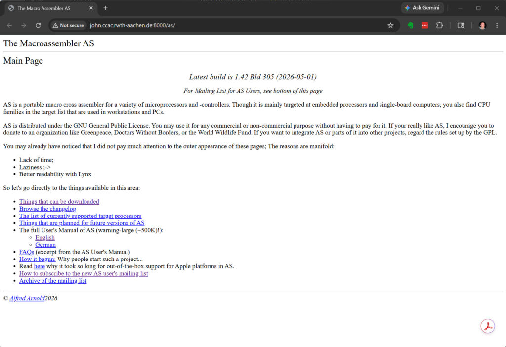
After trying various assemblers, ASL impressed me the most.
It supports a number of processors, including all of our 8-bit favourites.
Like the 6809, 6502, Z80, and also supports the 68K.
Also, it has a no-nonsense GNU General Public License.
So, You may use it for any commercial or non-commercial purpose without having to pay for it.
In addition, it continues to be updated, with the latest release being the same month that I wrote this blog (May 2026).
To help you out, I’ve also included my Visual Studio Code tasks.json file in the Digicool Things MECB github repository for this project.
This json file defines the build task I use for Assembling to both .bin and .s19 output files.
So, I’m all set for creating ROMable code, and code that can be transferred to RAM for running.
You will probably need to edit the json file for your own path preferences, but it should provide a helpful starting point.
Development Folder Structure
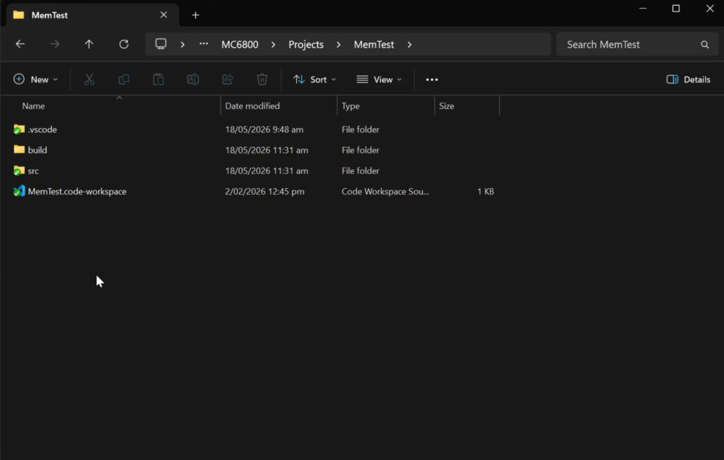
As an example, below you can see my folder structure for development.
For a full walk-through, be sure to watch the linked video.
Within my MC6800 personal repository folder, I have a Projects folder.
Within this folder I have a named folder for each project.
If I go into the MemTest folder, for example, I have my Visual Studio Code workspace file, and a .vscode folder that contains my tasks.json file.
Then I’ve created 2 additional folders. These are for my source code (src), and a build folder for the builds.
If I go into the src folder, I have my .asm source for the project.
Separate to this, I’ve also created an “include” folder, which also lives in the Projects folder, so I can put my common .inc files there, to make them available to all projects.
The tasks.json file (share on gihub), also includes the Assembler directive to point to my include folder.
Now, if I go into the build folder, I have 3 files from the last build task run.
There is both .bin and .s19 Assembler output files, and an Assembly listing file.
So, hopefully this example folder structure should be helpful with understanding my tasks.json file paths.
If you choose to use a similar folder structure, you may not need to change my tasks.json file at all.
MemTest Program Example
So, next, as an example of developing and running your own programs, I’ve created my own version of Emil’s MemTest program.
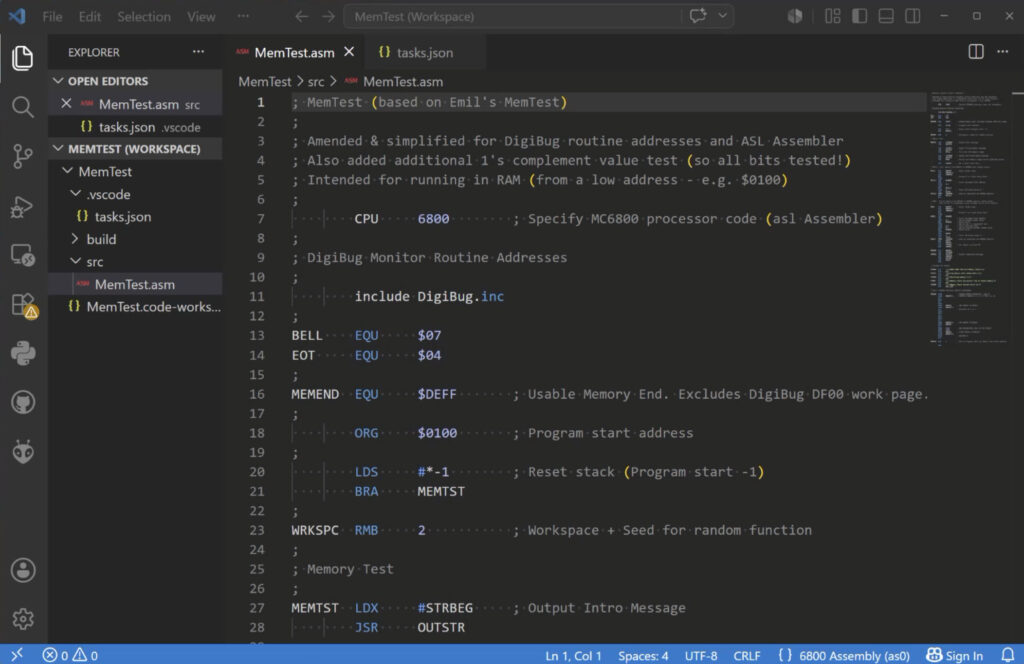
Essentially, I’ve simplified it to use our DigiBug monitor routines, and also added an additional “byte compliment” storage test, which ensures that all memory bits are being tested.
So, let’s take a look at the code. For a full walk-through, be sure to watch the linked video, otherwise…
The first code line specifies (for the ASL Assembler), that we want to assemble for the 6800 processor.
Then I have a couple of equates for the Bell and End Of Text EOT characters.
I then define the top of usable memory address for our 56K RAM system MEMEND, noting that the top 256 byte bank (at $DF00), is used by the monitor.
We could have tested right up to $DFFF, but I chose to stop at $DEFF.
Then we define our program start address in RAM at $0100
And, I initialise the stack to be in the memory bank below our start address (i.e. growing downwards from $00FF).
Again, this isn’t really necessary, as our DigiBug Monitor has already initialised the stack pointer.
Then, we jump over a 2 byte workspace, which I’ve allocated WRKSPC
And then we’re into the actual memory test code.
You’ll need to view the video, or load the .asm (from Github), as the following is on the next source page.
The actual test code simply outputs a couple of messages, and then calls the Memory Fill subroutine, to fill the memory with pseudo random bytes.
Then we output another message, and call the Memory Verify subroutine, to verify the memory we filled.
After this we exit to the Monitor’s warm start.
I’ll leave the rest of the code for you to read at your own pace.
Load / View / Trace & Run Programs
Finally, I display the Visual Studio Code Terminal and run the Build task, so that we’re ready to give it a try.
To see me walk-through the Loading, Tracing, and Running of our MemTest program, you’ll need to view this final chapter in the linked video.
Beyond this, have fun, and I do look forward to hearing about your experimentation and creations!
Be sure to join us on the Forum.