
- Pre-amble
- Introduction
- Update – Mon 29 Sept
- Update – Mon 6 Oct
- Update – Mon 13 Oct
- Update – Mon 20 Oct
- Update – Tue 28 Oct
- Finalising the CHIPOS ROM Code
- CHIP-8 Program Testing
- CHIP-8 Nostalgia
- Exploring the new 128×64 "Hi-Res" Capability
- Rediscovering my First Game
- DREAM 6800 CHIP-8 Machine Code Subroutines
- Correcting Machine Code Subroutines for the DREAM 6809
- The Big One – DREAM Invaders!
- Tape Program Directory
- Administration & Time to make a Video!
- Update – Mon 3 Nov – Home run!
- Update – Thu 6 Nov
- RetroChallenge 2025 – Project is Complete!
Pre-amble
This is (was) a late entry into RetroChallange 2025. As it happened, last year (2024) was the first time I’d entered RetroChallenge, and I thoroughly enjoyed the added incentive and structure that it encouraged with my retro project.
This year (2025), I completely forgot about RetroChallenge, however I just happened to be progressing another very RetroChallenge appropriate project in October, when I was reminded of RC2025.
Interestingly, I hadn’t been formally documenting my progress from the start of the month (something that RC2024 had encouraged me to do last year), so, with my raw notes to hand, I’ll now formally document my progress…
Introduction
Following on from last year’s 2024 RetroChallenge CreatiVision re-Creation project, I’ve been planning a re-Creation of the DREAM 6800 computer from the late 1970’s, using my flexible and configurable MECB based 8-bit retro computing platform.
DREAM 6800
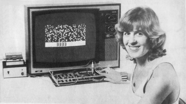
The DREAM 6800 was published in ‘Electronics Australia’ in 1979, and was my first hands-on microprocessor experience, as a young teenager.
RCA COSMAC VIP
The original DREAM 6800 was inspired by the RCA COSMAC VIP system, which originally ran a CHIP-8 language interpreter with a chunky graphics display. This combination was ideal for coding early video games.

DREAM 6800 (6809) re-Creation
For my DREAM 6800 re-Creation, I intend to move on to the 6809 (which was introduced around the same time).
I also plan to enhance the original 64×32 graphics to also provide a higher 128×64 resolution, as was also envisaged by the original creator.
In addition, I also plan to include other enhancements inspired by recent retrospective discussions of the original design, that I’ve had with the original DREAM 6800 developer, Michael.J.Bauer.
Otherwise, I plan to remain true to the original DREAM 6800 design intention and function, to re-Create the original DREAM 6800 experience.
Update – Mon 29 Sept
Michael.J.Bauer
As a pre-cursor to completing my new DREAM 6800 (6809) re-Creation project, I had already reached out to the original designer of the DREAM 6800, Michael.J.Bauer.
This was primarily to enquire about his website published comment regarding an alternative circuit, to replace the now hard to find NE566 Function Generator (or voltage-controlled oscillator), as used in the original design.
This lead to further email discussions, which also covered some retrospective on early design decisions.
Inspiration
The email discussions with Mike were very inspirational. One of the first inspirations, was Mike’s comment about potentially using a 4×5 matrix keypad to provide an additional row of 4 function keys. This would be instead of the original design’s hardware debounced single function key.
The CHIPOS operating system, which the DREAM 6800 implements, uses the single function key in combination with the 0 – 3 hex keys, to implement 4 different functions. Function 0 through Function 3.
So it did seem a logical enhancement to instead provide 4 dedicated function keys, implemented as an additional row of the scanned keyboard matrix, with software debounce (also avoiding the need for hardware debounce components).
4×5 Matrix Hexidecimal Keypad
With 4 dedicated Function Keys in mind, one of my pre-cursor projects and the subject of my most recent video (at the time of writing this), in mid-September, was a new Hexadecimal 4×5 Matrix Keypad, to enhance my existing 4×4 Matrix Keypad.
OLED Display 128×64
In the month prior (August), I had completed a project to add a 128×64 OLED display Card to my MECB platform.
This 128×64 OLED Display Card project did in fact prompt the original inspiration for my now DREAM 6800 (6809) re-Creation project.
There was also a sneak preview at the end of the OLED Display Card video, where I’d already started to experiment with the OLED display with some existing code.
So, at this point (end of September), I was finally ready to make use of these two prior projects, to now dive fully into my latest retro system re-Creation (based on the original DREAM 6800).
Update – Mon 6 Oct
CHIPOS 6800 to 6809 Conversion
For the first week of the October RetroChallenge 2025 I started with completing the initial work of fully converting the original DREAM 6800 CHIPOS operating system source code, to instead be 6809 Assembly code (originally 6800), and to also be compatible with my preferred asm6809 assembler.
With this 6809 conversion task completed, I quickly came to the conclusion that for further software development, including the changes necessary to support the new 4×5 Matrix Hex Keypad, I’d (of course) need to get the Keypad connected!
Interface Circuit Design
So, at this point, I put the software development aside and focussed on designing a circuit for the additional interfaces required for my DREAM 6809 re-Creation.
This is basically for everything that connects to the DREAM’s MC6821 PIA. This comprises the Hexidecimal Keypad interface, a Sound interface (for speaker “bleeps”), and the Tape Input / Output interface (for saving and loading programs).
Hard to Obtain 70’s Components
As alluded to earlier, several of the IC components, that were used back in the original 1978 / 79 design, were now very hard (or expensive), to source. Therefore, a new circuit design, using currently available componets, was required.
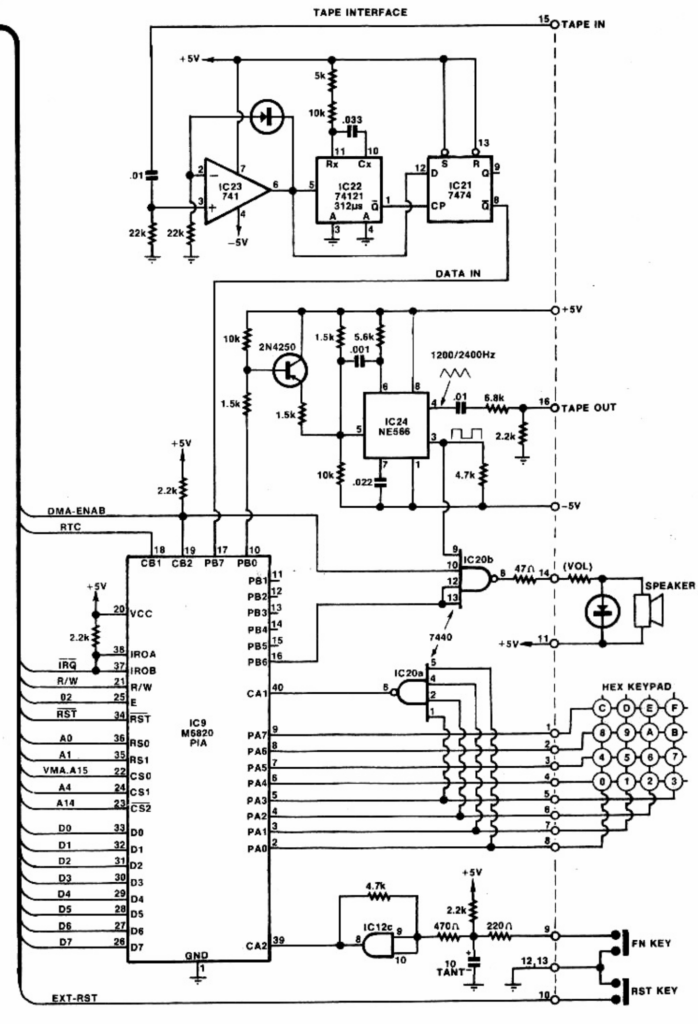
As you can see from the original Interface Schematic, it uses the now very hard to find NE566 Function Generator, a 741 dual supply op-amp, as well as a 7440 dual 4-input NAND gate, and a 74121 Monostable Multi-vibrator.
The 74121 is still available, but it’s now relatively expensive.
In addition you can see the choices used back in 1978 / 79 for hardware debouncing a standalone single function key (FN).
Note also, that the original circuit used a dual-supply of +5V and -5V for both the TAPE IN and TAPE OUT interfaces.
Currently Available Components & Single 5V Supply
So, with consideration to currently available components, a single 5V supply desire, and email discussion with Mike (the original DREAM 6800 designer), regarding his proposed NE555 replacement (for the NE566), an initial schematic design was devised.
Initial v1.0 Schematic and PCB Design
In addition to drawing up my prototype v1.0 schematic, and ordering any parts needed to allow building and testing the design, I also started on the PCB layout for v1.0
Now, some might say that I never learn, as without any doubt a PCB designed before proving a circuit, is bound to create some level of wasted effort.
However, I have also learned that, in modern times, you can speed-up a project’s design path by taking on the risk of designing an unusable PCB. Sure, you might end up having to completely re-route a significantly changed circuit design, but on the positive side, you are forging ahead with establishing a first-cut of the project’s final PCB layout and also getting more experience with PCB routing!
Update – Mon 13 Oct
So, with components arriving from suppliers, and a completed layout for a v1.0 PCB, the second week of October was mostly spent on prototyping and testing the v1.0 schematic design.
v1.0 Not Working as Envisaged
Needless to say, not everything worked as envisaged!
The initial plan for a NE555 replacement circuit for the 566 did not operate as intended.
Also, my quick drawing-up of the LM386 amplifier circuit forgot that the LM386, by default, implements a gain of 20 (something I really should just know).
In addition, the original plan for digitally controlling the sound (speaker) output, unfortunately did not have the effect of fully turning-off the sound. There was some residual sound still evident when the sound was switched-off, which also related to the amplifier’s default gain of 20.
Testing & Designing v2.0 Schematic
Therefore, much of the week was involved in the testing and re-designing the schematic, and also ordering more parts!
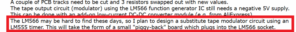
The good news is that by the end of the week I now had a (mostly) working prototype. I say “mostly” as I just need one more component to finalise the NE555 replacement circuit.
The required component is a bilateral switch, to enable digital FSK frequency switching, whilst retaining a preferred 50% duty cycle!
My search for an appropriate solution resulted in me finding a very nice / compact (as in retro compact) DIP8 packaged single bilateral switch, for the necessary bidirectional current switching.
Once this final component arrives, I will be able to do the final proof of the circuit in operation, to allow moving on to re-routing (and ordering), the new v2.0 PCB design.
Re-routing the PCB for v2.0
Re-routing the PCB was going to be a big job, as it turned out that my final v2.0 schematic actually beared little resemblance to my original v1.0 schematic.
It seemed that most parts of the circuit underwent some design change to correct the design flaws, in addition to design changes like implementing the previously unused 74HCT74 2nd flop-flop as a new means of digitally controlling the sound output.
However, the good news for the end of the second week was that a final release v2.0 circuit was now (mostly) proven, and the v2.0 PCB re-routing was underway!
More importantly, I now had a mostly working prototype. This enables me to return to the CHIPOS Assembly Code changes for my DREAM 6809 (re-)creation, as I now have a connected Keypad and Sound system.
Update – Mon 20 Oct
As indicated in my last update, my 3rd week of October started with me waiting on a part (to enable the final testing of my new v2.0 schematic).
So, I started the week by working on completing the v2.0 PCB layout changes and re-routing. This was important, as I wanted to be able to submit my PCB manufacturing order, as soon as the final part arrived and I was able to complete the final circuit test.
CHIPOS Code Changes
With the PCB routing completed, I then dived back into the Assembly Coding aspect of the project. Numerous changes to the CHIPOS source code were required, to support the changes to the hardware design.
Firstly, the entire memory mapped graphic display was being replaced with drivers for the OLED panel display.
A small note here is that the use of a parallel 8-bit display panel was critical, as only the parallel interfaced panels allowed the reading of the internal display buffer contents. Serial attached panels only allow the writing of display data, therefore would require an external memory buffer to be maintained (as CHIP-8 implements an exclusive-or pixel display function).
Secondly, the removal of the PIA’s CA1 trigger for a Keypad key press, required a re-work of the keypad scanning code. As did the implementation of a 5th matrix row for 4 new function keys!
In addition, I desired to implement a new higher resolution font alternative, to take advantage of the new ‘Hi-Res’ 128×64 display mode. Effectively adding a smoother 6×10 font to the existing chunky 3×5 font.
Also, I had plans to utilise the new added function keys to enable a new way of exiting the “Memory Modify” (memod) mode, via the press of an alternate function key, as opposed to the original requirement to use the system Reset.
In addition I had plans to change the user notification of Tape Dump & Load progress (start & end of Dump / Load). On the original DREAM 6800, tape Dump / Load progress was signified by turning-off the display (disabling DMA), during tape operations. This was required for timng reasons. Whereas, with our new OLED display, no DMA microprocessor interruption is necessary, so we can do something tidier for Dump / Load completion notification.
It’s worth also noting here, that Mike was originally limited to the 1K ROM space of the original 2708 EPROM which held his CHIPOS operating system, meaning that he was forced to improvise to get the full code to fit in the 1024 bytes available. Therefore he had to get creative and also accept a few limitations, in order for the code to fit within the available 1K ROM space.
One aspect of this creativity was that Mike implemented a compressed font, which in combination with an efficient decompress routine, saved on ROM space. I no longer needed this type of ROM space saving, so I instead went for a more straight-forward simple font image table.
Fortunately, the 1K ROM space limitation is now a thing of the past, and we can be more focussed on function instead of available space!
Finally, I intend to add an additional CHIP-8 instruction, to allow setting the display mode (either the original 64×32 or the higher resolution 128×64), from within your CHIP-8 program.
So, as you can see from the above initial list, I have a bit of coding to do!
Arrival of Final Component & v2.0 Testing Success
Before the week ended, my final part arrived, and I was able to quickly prove that my v2.0 circuit was successully operational.
With this, the v2.0 PCB order was placed, so I therefore finished the third week now awaiting the arrival of my PCB order!
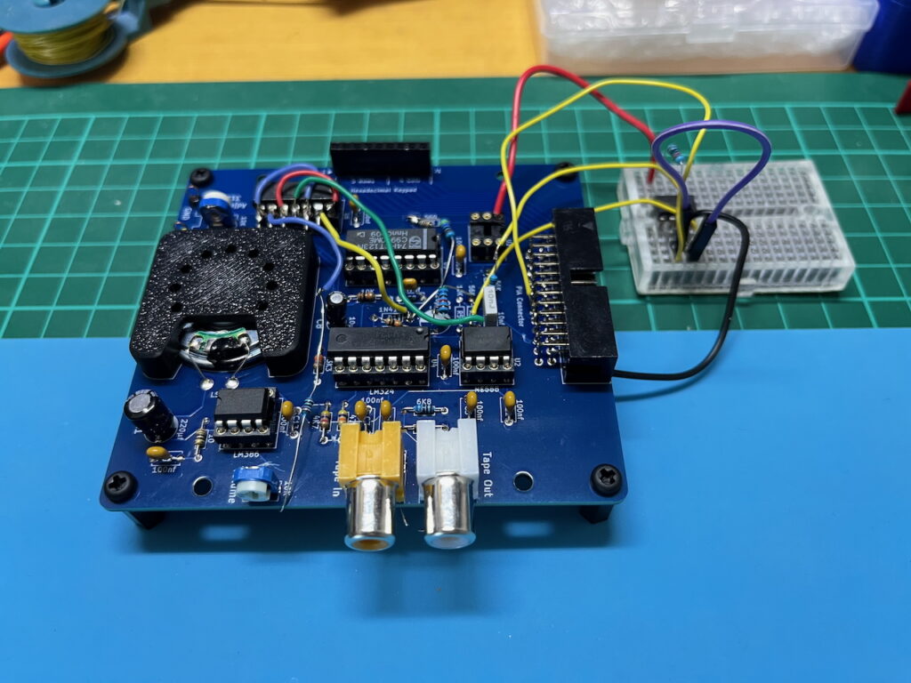
Final v2.0 Prototype (on a v1.0 PCB and breadboard)
Just for interest sakes, below is a photo of my fully working prototype. It’s a (very) heavily modified v2.0 creation, on an initial v1.0 prototype PCB base (and small breadboard).
Needless to say, there is just as many cut-tracks and jumper-wires underneath the v1.0 PCB!
It’s interesting, as there will always be debate over whether it’s quicker to just breadboard the entire circuit, to start with (as we always did in earlier days), or, to start with an inital PCB design for your first full prototype.
With modern PCB design tools and inexpensive prototype PCB manufacturing, I’m now in the camp of prototyping a final design via a prototype PCB, instead of on breadboard(s). Mainly for the reasons I alluded to earlier.
However, I do still use a breadboard for testing small circuit segments, just not for full project designs.
Update – Tue 28 Oct
With the v2.0 shematic now successfully tested, and v2.0 PCB’s designed and ordered, the 4th week of October started off with finalising the CHIPOS code changes for my initial release.
Finalising the CHIPOS ROM Code
Finalising the CHIPOS code also included moving the beta “final” code to ROM space, whereas during development it was being assembled into RAM space (to simplify the test cycle).
As a result I have now positioned the CHIP-8 interpreter to be executed from memory location $C800.
The original DREAM 6800 had the CHIP-8 interpreter executing from $C000 (effectively from the start of the ROM), however my DREAM 6809 (re-)Creation has it’s standard MECB mapped I/O bank located between $C000 – $C0FF, making these 256 bytes (essentially at the beginning of the ROM space), unusable for ROM code.
Also, it seemed quite intuitive to have a CHIP-8 program run by executing from C800 instead of C000 (as-in, CHIP-8 = C8).
CHIP-8 Program Testing
So, having achieved a tested (and ROM located) CHIPOS implementation for my new DREAM 6809, it was time to dive into some actual use of the system, to further test operation.
Exciting times!
The first thing I did was to enter a couple of the sample CHIP-8 programs which were published in the original 1979 ‘Electronics Australia’ project article.
These programs comprised of a relatively simple countdown timer (counting down and decimally displaying, every second, starting from a count of 250), and, also a random bitmapped pixel display sequence that demonstrated the Exclusive-Or pixel update feature of CHIP-8.
CHIP-8 Nostalgia
So, I keyed these CHIP-8 programs in via the Hex Keypad (just like we did in the old days), run the CHIP-8 programs, and also tested saving the programs to Tape, and re-loading them again from Tape (again, just like we did in the old days).
It was a very nostalgic experience!
Exploring the new 128×64 “Hi-Res” Capability
My next step was modifying these original 64×32 display programs to utilise the new “Hi-Res” 128×64 display.
This actually was pretty straight-forward as all I needed to do was change the X & Y coordinates and coordinate range references, and also (for the countdown timer), change the vertical font display height from 5 pixel rows to 10 pixel rows.
All displayed correctly, as planned, in my new 128×64 display mode.
These “Hi-Res” versions were also saved to Tape.
Rediscovering my First Game
I remember the first Computer Game that I ever wrote, was written in CHIP-8 on my DREAM 6800. I had called it “Dogfight“.
I also remember taking my DREAM 6800 into school and it being setup on the Science teacher’s desk for the class to play my “Dogfight” game. I still remember the excitement and interest it held, at a time when most people weren’t even aware of personal computing.
This program would have been lost, however fortunately it was published in “Dreamer” No.17 Jan ’82.
The “Dreamer” Newsletter was published in 19 issues, between September 1980 and 1982, providing support and shared programs for the users of the DREAM 6800.
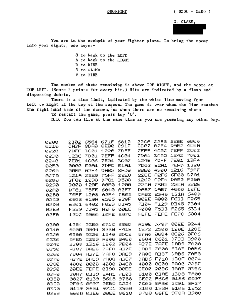
Having rediscovered my program listing in Dreamer No.17, I excitedly re-keyed it into my new DREAM 6809 (re-)Creation, to re-experience what I orginally wrote.
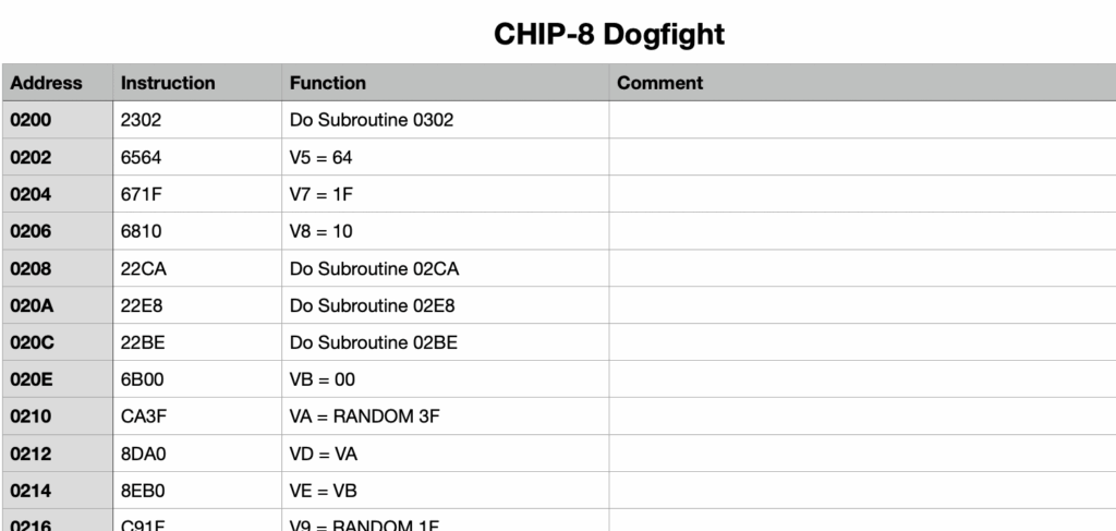
Interestingly, it didn’t work. So, to determine why, I manually “disassembled” the CHIP-8 program.
DREAM 6800 CHIP-8 Machine Code Subroutines
Having completed the “dIsassembly”, the reason for it’s failure became clear.
In writing the program, way back around 1980, I had made use of the CHIP-8 ability to call Machine Code subroutines.
As my DREAM 6800 re-Creation has been implemented on the newer, more powerful, 6809 microprocessor, the original machine code instructions were no longer compatible.
Firstly, because the 6809 is not fully binary compatible with the 6800. Secondly, the standard CHIPOS Subroutine addresses have changed.
To explain further, while converting the original CHIPOS code from 6800 to 6809, and also modifying the code for the new hardware implementation, the original “hardwired” call addresses have (of course) changed.
To ensure any further changes to the CHIPOS code does not again change published standard subroutine calling addresses, I took the approach of creating a fixed address Jump Table for all of the published CHIPOS subroutines.
This will solve the issue going forward. It’s also worth noting that adding a subroutine jump table wasn’t possible in the original CHIPOS implementation, simply due to the limited space in the original 1K ROM (as explained earlier).
In addition, the op-codes of some 6809 instructions have changed, from what they were in 6800. In some ways, it’s actually surprising how many op-codes are unchanged, even though the instruction mnemonics have changed.
e.g. An A accumulator immediate load instruction was LDAA #$3C on the 6800, but on the 6809 it is now LDA #$3C
Despite this change in Assembly Code nmemonics, the op-code for an immediate data load of Accumulator A, is still $86
This is similar for all of the 8-bit Accumulator instructions. However, the op-codes for loading the X Index register has changed.
e.g. The immediate data load of the 16-bit X index register was $CE on the 6800, but is changed to $8E on the 6809.
Correcting Machine Code Subroutines for the DREAM 6809
As explained above, in order to solve the failure to run the “Dogfight“, it just requires me to locate the Machine Code Subroutines, and amend the appropriate bytes for 6809 machine code, instead of the old 6800 machine code.
Below is an example of one of the identified Machine Code Subroutines, and in the right hand column are the byte changes needed, to correct the program to run on the 6809.
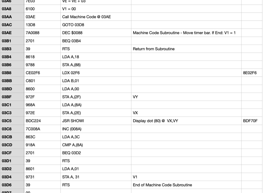
With a total of four Machine Code Subroutines located, and all amended for equivalent 6809 op-codes, my “Dogfight” game was finally up and running!
And, another surge of nostalgia! 🙂
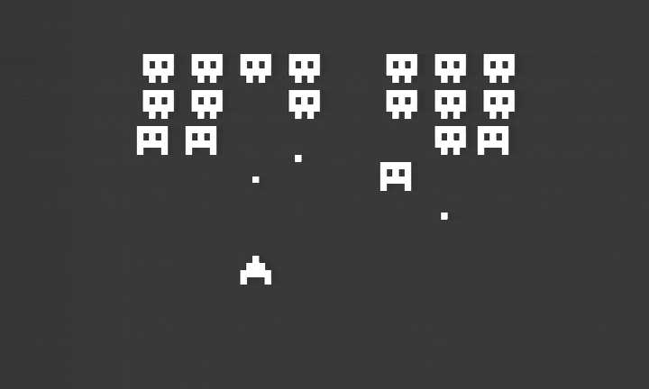
The Big One – DREAM Invaders!
So, having first played with and proved that CHIP-8 was functioning (as expected), on my DREAM 6809 (re-)Creation, and also still having some days to go before my v2.0 PCB’s would finally arrive, I decided I’d really love to try converting the original “DREAM Invaders“.
“DREAM Invaders” was a 2K 6800 Machine Code game, written by Michael.J.Bauer in 1980. It even required the original DREAM 6800’s 1K RAM to first be expanded (e.g. with an Electronics Australia Dec ’80 published 4K Memory Expansion board project), before you had the memory space required to load “DREAM Invaders”.
So, I dived into making this a bonus extra for my DREAM 6809 (re-)Creation.
First, I had to locate the source code, and then convert it to 6809 code, which was also compatible with my favorite asm6809 Assembler.
Secondly, I had to work through the code, to change any CHIPOS subroutine call addresses (as outlined earlier), to their new Jump Table addresses.
Finally, I had to identify any other code changes that were required, to support the hardware changes implemented on my DREAM 6809 (re-)Creation.
And, success!
I now had “DREAM Invaders09”, running on my re-Creation!
Awesome! A future challenge (for me, or somebody else), is to enhance DREAM Invaders to take advantage of the new 128×64 resolution possibilities.
In summary, week 4 was a very successful week of coding and enjoying the re-living of the original late 70’s DREAM 6800 experience.
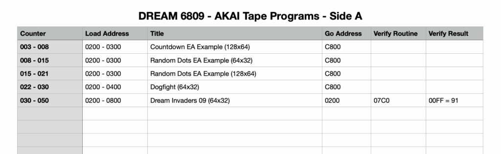
Tape Program Directory
I’ll finish-up my review of the last week, by showing a spreadsheet that I’ve created to track my program Tape saves.
Back in the original days, we (of course) had no built-in directory of our Tape program saves. So, it was necessary to make a manual note of the programs we had saved on Tape. The only reference we had was the Tape counter!
The following shows how I’m currently tracking my Tape saves in a spreadsheet. As you’ll note, the Dream Invaders program also includes a “Verify Routine”, that we can run to calculate a checksum (in this case stored at memory location $00FF).
This enables us to verify that the tape load was (likely), successful.
Administration & Time to make a Video!
All that remains (for sharing this project), is for me to now proceed with my administrative tasks of sharing the source code & resources (via github), and also making a Video to document my journey & demonstrate the operation.
This will be my focus for the coming week, which makes up the last days of October.
Update – Mon 3 Nov – Home run!
In the last days of October, the first part of my Video was filmed and edited.
However, I then took some time-out for formally documenting my full October month, which is what has appeared in the detail documented above.
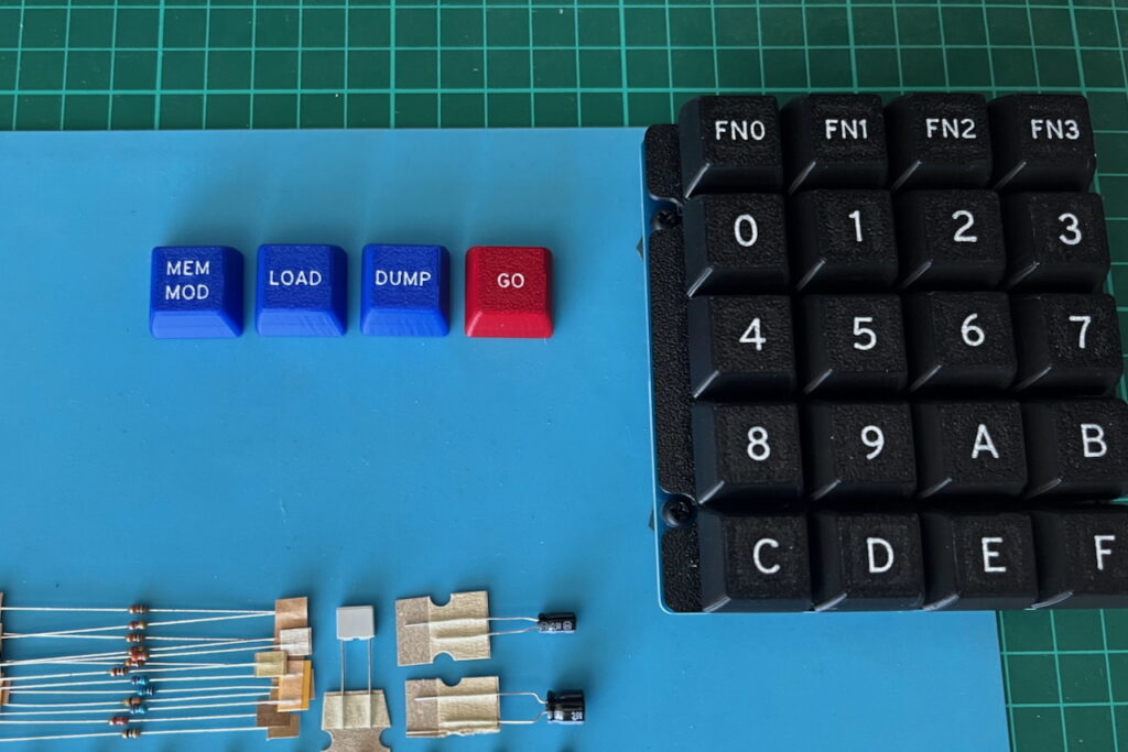
One Further Inspiration – Custom ‘Function Key’ Keycaps!
Then, I had yet another inspiration for one more (surely the last?), refinement to this project.
You see, someone wanted me to create some custom Function Key keycaps for their own project, using my 4×5 Matrix Hexadecimal Keypad.
This I happily did. But while doing creating their custom keycaps, it suddenly occurred to me that I should (of course), be doing the same for my own DREAM 6800 re-Creation project!
My 4×5 Matrix Hexadecimal Keypad has four generalised FN0 – FN3 labelled function keys. Which (clearly), were inspired by, and align with, the original DREAM 6800’s four [FN] [0] through [FN] [3] commands.
But, I will admit that while using my new DREAM 6809 (re-)Creation, I did occasionally have to double-check whether FN1 or FN2 was the “Load” command (or the “Dump” command)!
Clearly this confusion could be resolved by using the fact that we now have four individual function keys, to simply create custom keycaps that clearly reflect the four commands themselves.
I mean, it really is truly amazing how something seemingly this obvious, requires external inspiration, to bring it to your attention.
Anyway, what I have now created is some more appropriate DREAM MX keycaps for the four function keys. Clearly labelled for the four CHIPOS commands: Memory Modify MEM MOD, Tape Load LOAD, Tape Dump DUMP, and Go GO.
Also, colour coding these new keycaps, to contrast the command keys from the regular 4×4 Hexadecimal Key matrix.
Here are what they look like (before I fit them to the Keypad, replacing FN0 – FN3):
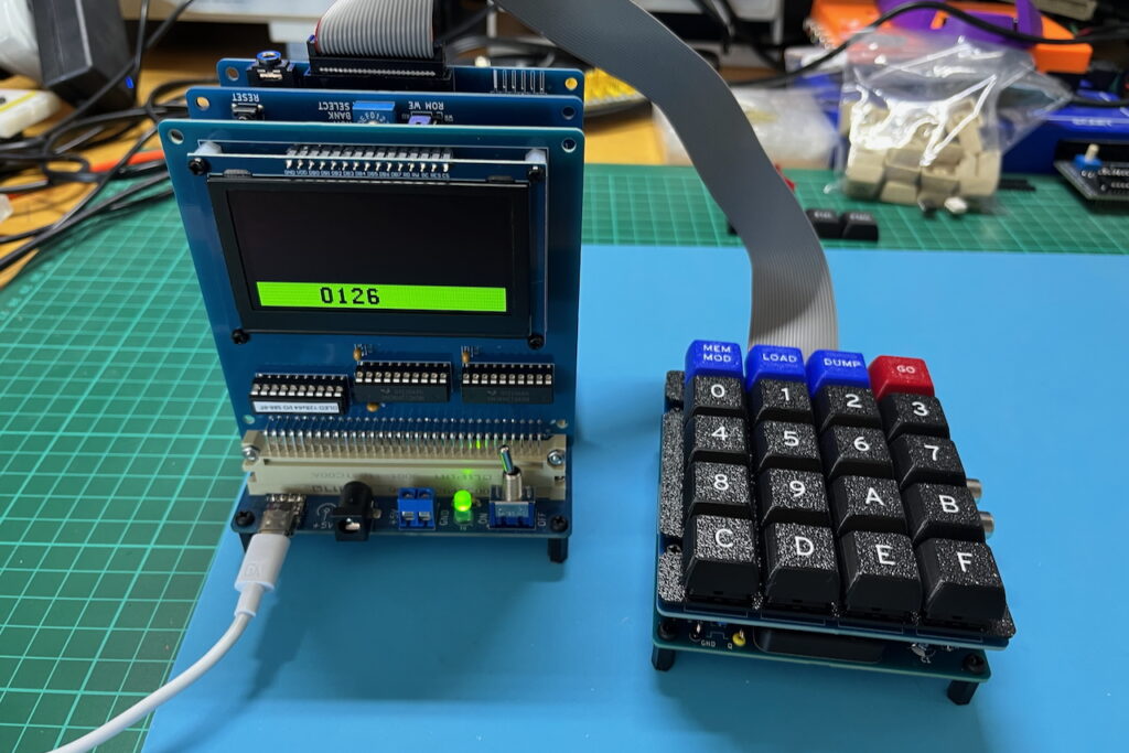
The Finalised DREAM 6809 (re-)Creation
So, with the (last?) refinement to my DREAM 6800 re-Creation project now complete, and the final version (v2.0) now up and running on a production ready finalised PCB, it was time to finally get back to working on my Video.
But just before I do, here’s a photo of the final completed project, in use!
Update – Thu 6 Nov
I’ve spent the last few days filming and editing the project video, only to realise that before even getting into reviewing the code and demonstrating the use of the system, I’m already approaching 30 minutes in video length!
Project Video being Released in 2 Parts
I want to do this project the justice it deserves, but I also don’t want to inflict an hour long video on anyone!
So, I’ve just today (Thu 6 Nov), made the decision to split the video into 2 parts, with Part 1 being published this weekend.
The good thing is, this does mean the first Video will be released sooner (than otherwise).
It also means that I can get on to the sharing of resources (github, Tindie etc.), while temporarily parking the editing of Part 2 (briefly).
This RetroChallenge blog has also provided a good alternative (to the Video), for capturing my overall project journey.
RetroChallenge 2025 – Project is Complete!
DREAM 6800 (6809) re-Creation – Video/Blog/Resources
Part 1 can be found here: DREAM 6800 (6809) re-Creation – Part 1
Part 2 can be found here: DREAM 6800 (6809) re-Creation – Part 2
As usual, you’ll find all the resources, including all source code, on my Github repository for this project.
You’ll also find binary ROM images (for the different MECB 6809 CPU Cards), in their appropriate folders on the MECB Github repository.
And, if you’d like to support me, please do consider looking at the PCB’s and kitsets available from my Tindie store.