
The first Card that I designed for MECB, was my original Prototype Card.
I had originally intended to also create a second Prototype Card with a PLD present, for prototyping with the glue logic already taken care of (mirroring the KiCAD MECB template).
So, better late than never! I also roll-in improvements based on feedback and a Forum member’s excellent work. These improvements are also then rolled-back into the original Prototype Card v2.
Join me as I present the new and updated Prototype Cards, and test the new Prototype PLD Card.
The original MECB Prototype card was a simple grid matrix card, intended for either point-to-point wiring of components, or, perhaps even using Wire-wrap sockets, like we did for our one-off designs back in the 70’s and 80’s.
In reality, I’ve mostly used the existing Prototype Card for bringing out the Bus signals to the easily accessible headers, for jumping across to a traditional breadboard for testing new circuits.
As noted, it was always my intention to make a second prototype Card, which would include a standard MECB glue-logic PLD on-board.
This would effectively mirror my original KiCAD Template, which includes a pre-routed PLD chip on the template PCB, to fast-track new MECB I/O Card PCB design.
Currently, when using the original Prototype Card to design a new peripheral Card, you usually need to start by wiring up a PLD (or some other glue-logic alternative), to allow generating your Chip Select signals for your new design.
In addition to this, I also received some helpful feedback for the original prototype card. This included the suggestion that both power and ground rails should be included on each side of the prototyping area (instead of just a power rail on one side and a ground rail on the other).
More recently, one of our active Forum posters (Clive), shared his latest Prototype Card design, which included the PLD. Clive also cleverly laid out the grid using 3-hole-long strips, which allows you to insert either 0.3″ or 0.6″ wide DIL packaged IC’s, with each side of the chip being connected to an additional row of connected holes, for easier wiring options.
Clive’s design actually prompted me to review my own early Prototype Card design, and reminded me to get-on with doing what I had originally intended.
Now, although I do like Clive’s design, we all have our own preferences. For me, I wanted the PLD Prototype Card to have room for a Zero Insertion Force (ZIF) socketed PLD. On the basis that for a Prototype Card, I’m more likely to be constantly removing the PLD for re-programming.
I also wanted to retain a few rows of plain non-connected grid holes along the top edge of the Card, to allow for easily mounting any desired 0.1″ grid based connectors.
So, I started re-designing a new Prototype Card, starting off from my KiCAD Template (as usual).
Lets take a look at what I’ve ended up with.
Here is the 3D render of the new PLD populated Prototype Card. Or, Prototype PLD Card (as I’ve called it).
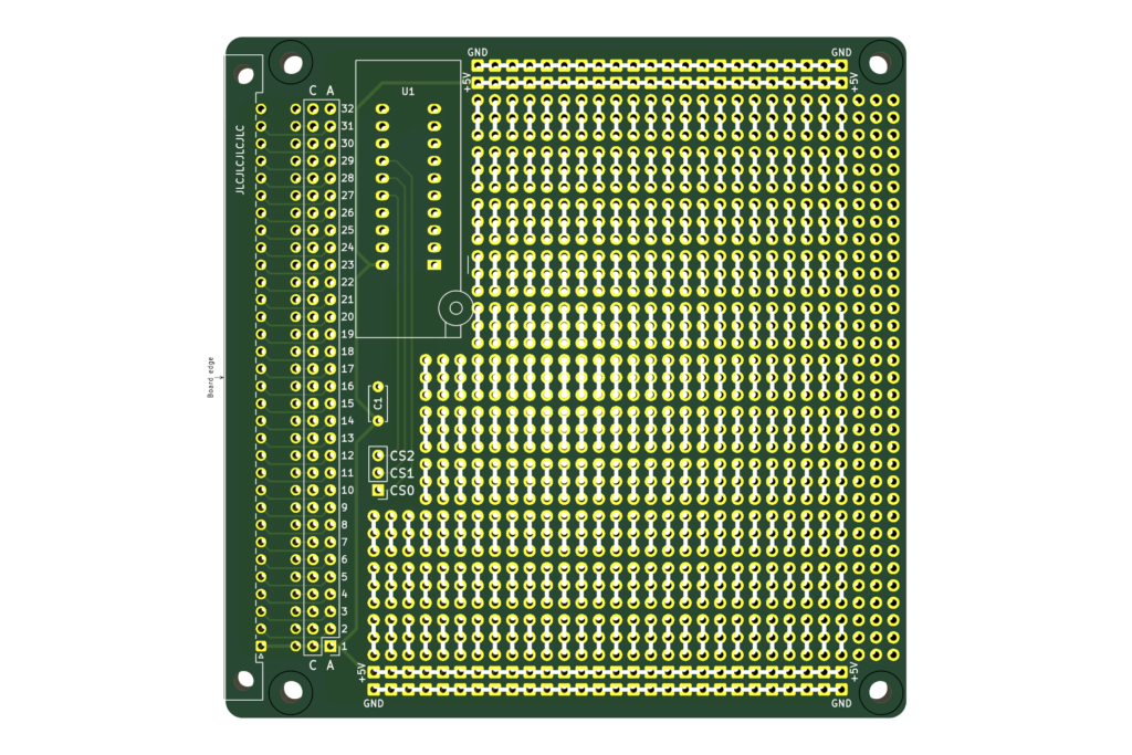
As you can see, the first key feature is the PLD, which uses a Zero Insertion Force (ZIF) socket footprint, to reserve the required extra space a ZIF needs.
I’ve then positioned a bypass capacitor and a 3 pin header for the PLD generated Chip Selects, so they don’t interfere with mounting a Zero Insertion Force socket.
In addition, you’ll note that I now have both 5V and Ground rails along each opposite edge, with the Ground rails along each outer edge.
The remainder of the Card is populated with connected strips that are each 3 holes long, with the exception of the last 3 rows at the Card “top edge”, which are a simple non-connected hole grid.
I’ve also clearly indicated all the connected holes, for both the power rails and prototyping grid, via silkscreened lines, on both sides of the PCB.
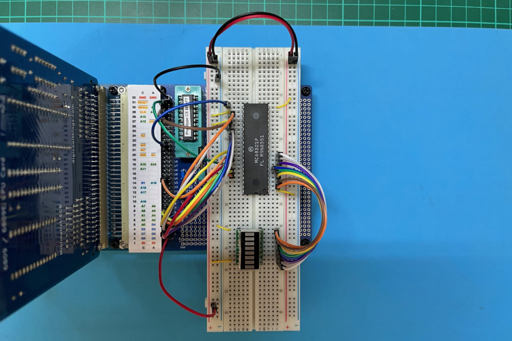
Be sure to watch the video, if you’d like to see the Prototype PLD Card in use, as I test it with a breadboard mounted PIA and “8-bit LED Thing”!
So, that’s my new Prototype PLD Card v1.0, which you’ll now also find on my Tindie Store.
Available either as just the PCB, or with optional Hardware & Component Packs, to fully complete your Prototype Card Kitset. This includes an option for a programmed PLD with Zero Insertion Force socket.
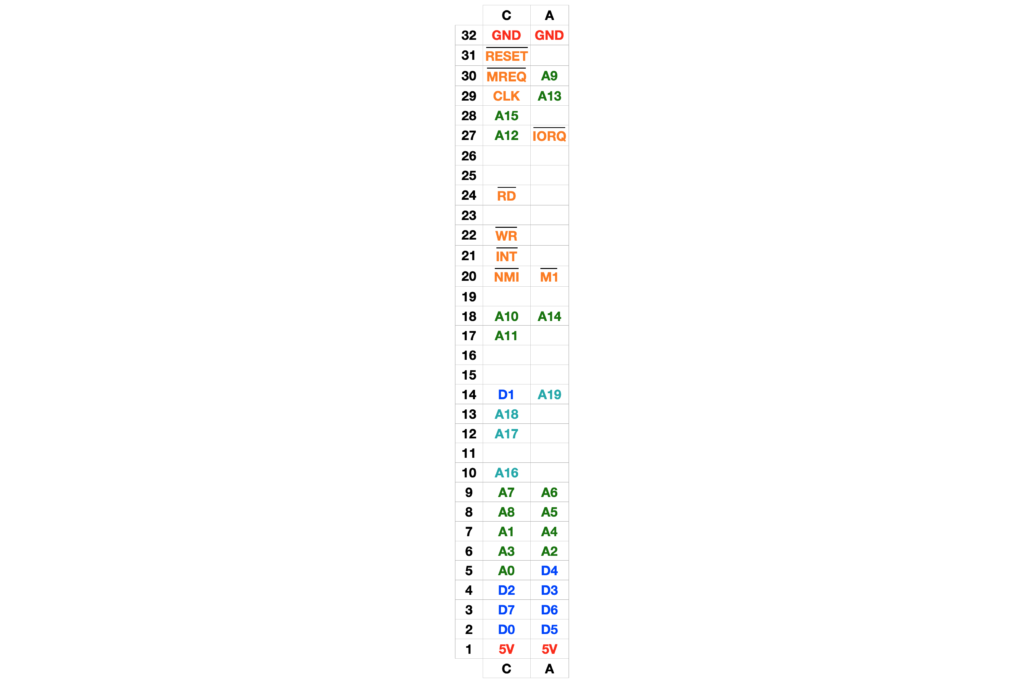
Note that if you order a full Kitset (PCB with both of the optional packs), then I’ll include a bonus of a laminated colour pin-out guide, sized to allow gluing onto the side fo the DIN41612 connector, for quick & easy reference!
Having now finally delivered on my original intention of making a PLD populated Prototype Card, complete with improvements based on original card feedback (and also Clive’s example), I then also took the opportunity of rolling the changes back into a v2.0 of the original full non-PLD Prototype Card.
So, here’s a 3D render of the v2.0 non-PLD Prototype Card.
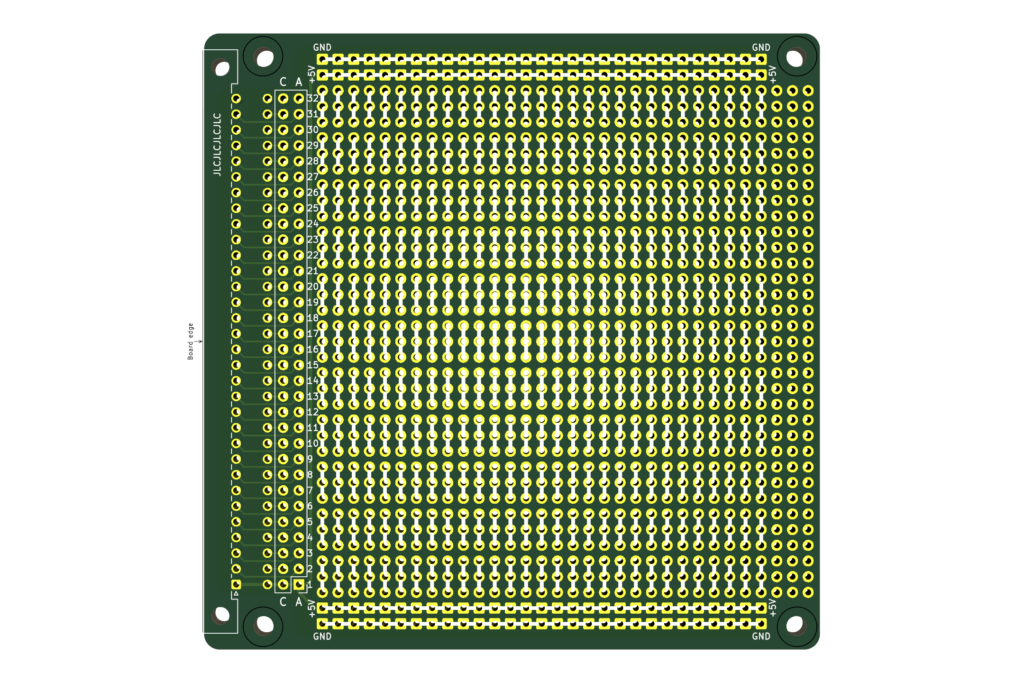
As you can see, it reflects all the improvements of the PLD Prototype Card, but simply replaces the PLD chip with a fuller grid of Prototyping space.
With these improvements, I’ve now also updated the existing Tindie Store Prototype Card listing, to now reflect this new v2.0 upgrade.
Hopefully, the improvements, and the finally delivered option of an alternative Prototype Card with a PLD, now provides improved Prototyping options to help with your own MECB experimentation!