6809 Angel

User avatar
djrm
Posts: 71
Joined: Wed Aug 21, 2024 9:40 pm
Location: Rillington / UK
Contact:

6809 Angel

Post by djrm »

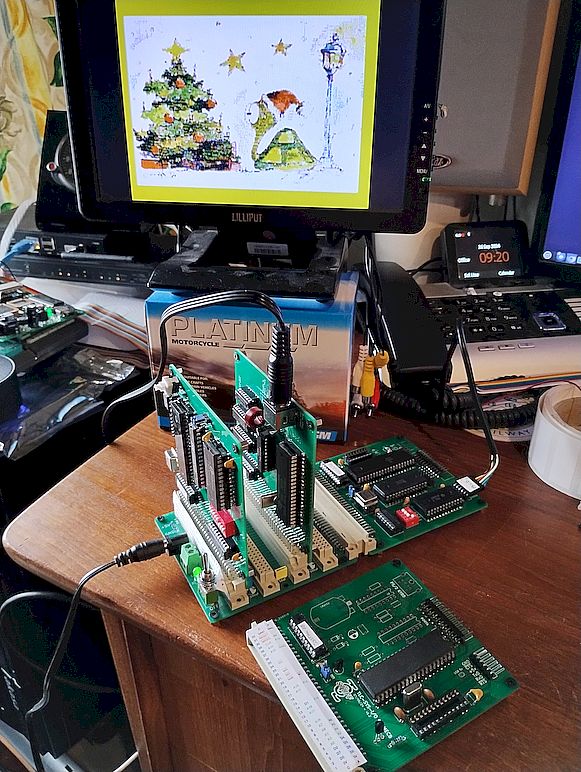
My original 6809 system 'Angel' from the late '80s is proving difficult to repair and not having any means to test the components I decided to build myself a new MECB based system, partly because I like the look of them but also to build a test harness for some of the component parts.

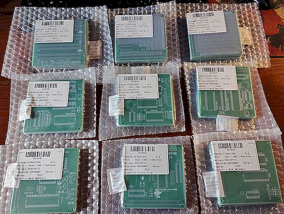
First off I ordered a set of boards and some custom components. I have been collecting various parts for this for some time, but still needed a few more bits and pieces too, clock generators and crystals were last to arrive here. The boards took just under one week from deciding to place an order to having them delivered from JLCPCB.
Image

I started with the 6809 CPU and Motorola I/O cards and when these started to work I built a TMS9918 and the TLS SYS I/O board. I was very happy when I ran the Christmas video and sound demo. I have the 6522 working too. I have no software to try the SCC2691 yet so this bit will have to wait.
Image

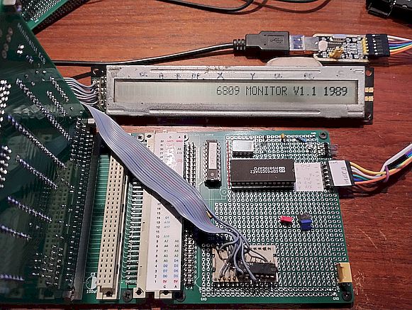
For testing the Angel components I have built a prototype card to interface an HD44780 LCD display and 6551 UART. debugging this card took a day, a couple of faults were fixed. firstly I had to include the 'E' clock into the address decode for the display, and secondly I has the 'A0' and 'A1' address bus signals swapped. The LCD is showing the sign-on message from my old monitor initialisation code.
Image

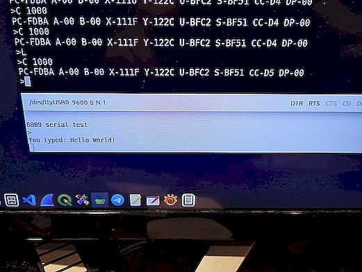
What I have found out is that the original UART, a 6551 is broken. The replacements are working 65C51 (but with txd bugs). I have test software running with both and some old 6551 on order. Here showing what I typed on a seperate serial port when the test program was run.
Image

Before the system was built I patched Greg's ASSIST09 monitor with the Disassembler to use the 6840 single step feature. I added a feature to show the next instruction during tracing, a bit handy when following listings etc.

Code: Select all

>R
PC-F842 A-00 B-00 X-20FE Y-E002 U-BFC2 S-BF51 CC-D4 DP-00 
PC-1000
>.OP-34 16        PSHS  X,B,A
PC-1061 A-00 B-00 X-20FE Y-E002 U-BFC2 S-BF4F CC-D4 DP-00 
>.OP-30 8C AD     LEAX  $AD ,PCR
PC-1063 A-00 B-00 X-20FE Y-E002 U-BFC2 S-BF4B CC-D4 DP-00 
>.OP-BF 10 15     STX   $1015 
PC-1066 A-00 B-00 X-1013 Y-E002 U-BFC2 S-BF4B CC-D0 DP-00 
>.OP-35 96        PULS  PC,X,B,A
PC-1069 A-00 B-00 X-1013 Y-E002 U-BFC2 S-BF4B CC-D0 DP-00 
>.OP-20 43        BRA   $1047 
PC-1002 A-00 B-00 X-20FE Y-E002 U-BFC2 S-BF51 CC-D0 DP-00 
>.OP-34 16        PSHS  X,B,A
PC-1047 A-00 B-00 X-20FE Y-E002 U-BFC2 S-BF51 CC-D0 DP-00 
>.OP-30 8D 00 B4  LEAX  $00B4 ,PCR
PC-1049 A-00 B-00 X-20FE Y-E002 U-BFC2 S-BF4D CC-D0 DP-00 
>.OP-A6 80        LDA   ,X+
PC-104D A-00 B-00 X-1101 Y-E002 U-BFC2 S-BF4D CC-D0 DP-00 
>.OP-E6 80        LDB   ,X+
PC-104F A-06 B-00 X-1102 Y-E002 U-BFC2 S-BF4D CC-D0 DP-00 
>.OP-8D 74        BSR   $10C7 
PC-1051 A-06 B-30 X-1103 Y-E002 U-BFC2 S-BF4D CC-D0 DP-00 
>.OP-7D C8 E0     TST   $C8E0 
PC-10C7 A-06 B-30 X-1103 Y-E002 U-BFC2 S-BF4B CC-D0 DP-00 
>.OP-2B FB        BMI   $10C7 
PC-10CA A-06 B-30 X-1103 Y-E002 U-BFC2 S-BF4B CC-D8 DP-00 
>.��


In the screen capture above you can see the debug crash and some garbage appear on the screen, this was happening with the original 2k Assit09 version too, something to investigate. An enhancement I'm thinking of adding is Assis09 trap decoding to help disassembly through system SWI calls. The problem seems to be related to tracing through I/O access instructions maybe some unexpected interaction happening here.

Next I'll maybe try and get my old keyboard working, it depends on having a 6522 available. When some more glue chips arrive I can try the 6502 board and test the SCC2691.

nb, I used some alternative components from stock for the CPU board. The RAM is is a 61c1024-15, for this I needed to tie pin 31 to Vcc to use the top half of its address space. The system rom is a flash part W27C512 set to RO with the jumper, again to use just the top half of address space. I found some old 6809s on ebay this week which I bought, one is a 'C' part som some speed test are in order...

Best regards, David.
User avatar
Editor
Posts: 246
Joined: Fri Nov 17, 2023 10:36 pm
Contact:

Re: 6809 Angel

Post by Editor »

Hi David. Thanks for posting! It's awesome to see someone else's journey, assembling their own custom system.

It's also good to see someone else making great use of the Prototype Card for hooking up some new hardware.
I'm pretty sure I have a very similar looking recovered HD44780 LCD display in one of my parts boxes, possible 2 lines of 40 chars? So, I'm certainly interested in more detail on what you've put together.

I really like the ASSIST09 extension to add disassembly of the next instruction during tracing. This is brilliant, and would be very helpful when debugging!

I also got some of the SCC2691 based I/O Card PCB's manufactured, but I haven't assembled one yet as I've only got several PLCC versions of the SCC2691 currently in my stock. I still need to either order in some DIP versions, or possibly I'll just make a PLCC version of the PCB.

Looking forward to more. :geek:
User avatar
djrm
Posts: 71
Joined: Wed Aug 21, 2024 9:40 pm
Location: Rillington / UK
Contact:

Re: 6809 Angel

Post by djrm »

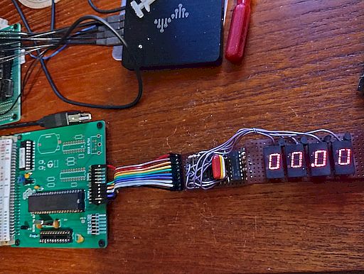
Today's endeavors have been to repair and code for this old home made multiplexed display which last ran on an original OSI C1P where it had various roles including RTC clock display and single step address display. It was connected to Port B on a VIA back then too with a similar interrupt timer doing the multiplexing. Next MECB experiment will be to try some C code and get VSCode working with the 6809 tools.
An unforeseen problem with the VIA was that I had only allocated 8 bytes I/O space to it so although the ports worked the timer and interrupt registers couldn't be written to, doh!
Image

My DIP SCC2691 came from AliEx, 5 for UKP 5, they are not completely dead but I haven't tried using them properly.

The 40 character is only single line, it was quite a disappointment when I first got it and it made the user interface quite difficult. It had to scroll horizontally. I think I have a two line 40 character display somewhere but the task for the C compiler will be to make a simple terminal using a larger display with T6963 controller.

The other thing I did was to write a 65c51 transmit function with timer instead of polling to circumvent the bug, I'll us this on my old board if I put a 65C51 chip in it but have some 6551 chips on order anyway. D
User avatar
djrm
Posts: 71
Joined: Wed Aug 21, 2024 9:40 pm
Location: Rillington / UK
Contact:

Re: 6809 Angel

Post by djrm »

After some head scratching I now have simple polled transmit and receive working on the SCC2691, I adapted the 6502 code I found here https://github.com/floobydust/C02-Pocke ... BIOS2b.asm
The code is complicated with the setup abstraction where the setup data is copied to ram before use, this is to allow the default settings to be in rom but alterable if needed.
This version is for use with my 6809 boards. The code listing is here, I'll study it some more and try optimising it one day ...

Code: Select all

                      ;******************************************************************************
                      ;       scc2691test.asm
                      ;
                      ;       A simple 6809 test for the MECB SYS IO Card with SCC2691 UART
                      ;
                      ;       This version is intended as RAM loadable code (eg. $1000 Entry).
                      ;       UART initialisation data is copied to RAM at 0x300 before use
                      ;       UART defaults to base address $C020
                      ;
                      ;       software sends '>' prompt then echoes received characters
                      ;       Assembled with asm6809 using invocation: 
                      ;       asm6809 scc2691test.asm -l scc2691test.lst -S -o scc2691test.s9
                      ;
                      ;       Author: djrm
                      ;       Date:   Sep 2024
                      ;
                      ;******************************************************************************
1000                                  ORG     $1000           ; should be ok in ROM or RAM
                      
1000  BD1029                          JSR     INIT_VEC        ; COPY SETTINGS TO RAM
1003  BD1041                          JSR     INIT_IO         ; CALL RESET AND INIT
1006  C604                            LDB     #%00000100      ;Get mask for xmit on
1008  F7C02A                          STB     UART_COMMAND    ;Turn on xmt
                      
100B  863E                            LDA     #'>'            ;SEND TEST DATA
100D  8D04            LOOP            BSR     TXDATA
100F  8D0D                            BSR     RXDATA          ;GET MORE TO ECHO
1011  20FA                            BRA     LOOP
                      
1013  F6C029          TXDATA          LDB     UART_STATUS
1016  C504                            BITB    #TxRDY
1018  27F9                            BEQ     TXDATA
101A  B7C02B                          STA     UART_TRANSMIT
101D  39                              RTS
                      
101E  F6C029          RXDATA          LDB     UART_STATUS
1021  C501                            BITB    #RxRDY
1023  27F9                            BEQ     RXDATA
1025  B6C02B                          LDA     UART_RECEIVE
1028  39                              RTS
                      
0300                  SOFTVEC         EQU     $0300   ;Start of soft vectors
                      ;******************************************************************************
                      ;SOFTCFG                EQU SOFTVEC+32  ;Start of hardware config parameters
0300                  SOFTCFG         EQU SOFTVEC     ;Start of hardware config parameters
                      ;Soft Config values below are loaded from ROM and are the default I/O setup configuration data that
                      ; the INIT_x routines use. As a result, you can write a routine to change the I/O configuration data
                      ; and use the standard ROM routines to initialize the I/O without restarting or changing ROM. A Reset
                      ; (HW or coded) will reinitialize the I/O with the ROM default I/O configuration.
                      ;There are a total of 32 Bytes configuration data reserved starting at $0320
0300                  LOAD_2691       EQU     SOFTCFG+00              ;SCC2691 SOFT config data start
                      ;******************************************************************************
C000                  IOPAGE          EQU     $C000                   ;I/O Page Base Start Address
                      ;******************************************************************************
C028                  SCC2691_BASE    EQU     IOPAGE+$28              ;Beginning of Console UART address
                      ;
C028                  UART_MODEREG    EQU     SCC2691_BASE+$00        ;MR1/MR2 same address, sequential read/write
C029                  UART_STATUS     EQU     SCC2691_BASE+$01        ;UART Status Register (READ)
C029                  UART_CLKSEL     EQU     SCC2691_BASE+$01        ;UART Clock Select Register (WRITE)
C02A                  UART_BRGTST     EQU     SCC2691_BASE+$02        ;UART BRG Test register (READ)
C02A                  UART_COMMAND    EQU     SCC2691_BASE+$02        ;UART Command Register (WRITE)
C02B                  UART_RECEIVE    EQU     SCC2691_BASE+$03        ;UART Receive Register (READ)
C02B                  UART_TRANSMIT   EQU     SCC2691_BASE+$03        ;UART Transmit Register (WRITE)
C02C                  UART_CLKTEST    EQU     SCC2691_BASE+$04        ;X1/X16 Test Register (READ)
C02C                  UART_AUXCR      EQU     SCC2691_BASE+$04        ;Aux Command Register (WRITE)
C02D                  UART_ISR        EQU     SCC2691_BASE+$05        ;Interrupt Status Register (READ)
C02D                  UART_IMR        EQU     SCC2691_BASE+$05        ;Interrupt Mask Register (WRITE)
C02E                  UART_CNTU       EQU     SCC2691_BASE+$06        ;Counter/Timer Upper Register (READ)
C02E                  UART_CNTUP      EQU     SCC2691_BASE+$06        ;Counter/Timer Upper Preset Register (WRITE)
C02F                  UART_CNTL       EQU     SCC2691_BASE+$07        ;Counte/Timerr Lower Register (READ)
C02F                  UART_CNTLP      EQU     SCC2691_BASE+$07        ;Counter/Timer Lower Preset Register (WRITE)
                      ;
                      ;******************************************************************************
0001                  RxRDY           EQU     1
0004                  TxRDY           EQU     4
                      ;******************************************************************************
1029                  INIT_VEC
1029                  DATA_XFER       ;SEI    ;Disable Interrupts, can be called via JMP table
1029  1A10                            ORCC    #$10            ;Disable Interrupts, can be called via JMP table
102B  108E0020                        LDY     #CFG_TABLEE-CFG_TABLE
                      ;               LDX     #$20            ;Set count for 32 bytes
102F  8E0020                          LDX     #CFG_TABLEE-CFG_TABLE
                      ;DATA_XFLP      LDA     VEC_TABLE-1,Y   ;Get ROM table data
1032  A6A9107D        DATA_XFLP       LDA     CFG_TABLE-1,Y   ;Get ROM table data
1036  A7A902FF                        STA     SOFTVEC-1,Y     ;Store in Soft table location
                      ;               DEY                     ;Decrement index
103A  313F                            LEAY    -1,Y            ;Decrement index
                      ;               DEX                     ;Decrement count
103C  301F                            LEAX    -1,X            ;Decrement count
103E  26F2                            BNE     DATA_XFLP       ;Loop back till done
                      ;               CLI                     ;re-enable interupts
                      ;               ANDCC   #$EF            ;re-enable interupts
1040  39                              RTS                     ;Return to caller
                      ;******************************************************************************
                      
                      ;
                      ;Initializing the SCC2691 UART as the Console
                      ;An undocumented bug in the W65C02 processor requires a different approach for programming the
                      ; SCC2691 for proper setup/operation. The SCC2691 uses two Mode Registers which are accessed at
                      ; the same register in sequence. There is a command that Resets the Mode Register pointer (to MR1)
                      ; that is issued first. Then MR1 is loaded followed by MR2. The problem with the W65C02 is a false
                      ; read of the register when using indexed addressing (i.e., STA UART_REGISTER,X). This results in
                      ; the mode register pointer being moved to the second register, so the write to MR1 never happens.
                      ; While the indexed list works fine for all other register functions/commands, the loading of the
                      ; Mode Registers needs to be handled separately.
                      ;
                      ;NOTE: The W65C02 will function properly "if" a page boundary is crossed as part of the STA
                      ; (i.e., STA $FDFF,X) where the value of the X register is high enough to cross the page boundary.
                      ; Programming in this manner would be confusing and require modification if the base I/O address
                      ; is changed for a different hardware I/O map. Not worth the aggravation in my view.
                      ;
                      ;The same bug in the W65C02 also creates a false read when sending any command to the Command
                      ; Register (assumed indexed addressing), as the read function of that hardware register is the
                      ; BRG Test register. This can result in a different baud rate being selected, depending on the
                      ; baud rate tables listed in the Datasheet. When using either 19.2K or 38.4K baud rate, the tables
                      ; are the same for both normal and BRG Test mode, so the UART will operate normally. Changing to a
                      ; different baud rate via the BRG Test register requires additional coding to use any of the
                      ; extended baud rates.
                      ;
                      ;NOTE: As a result of the bug mentioned above, the X1/X16 Test Mode register will be toggled twice
                      ; when the INIT_2691 routine is executed. The end result is the 2691 UART is correctly configured
                      ; after the routine completes. Also note that the NMI PANIC routine above also toggles the X1/X16
                      ; Test Mode register in case it was inadvertantly invoked (toggled).
                      ;
                      ;There are two basic routines to setup the 2691 UART
                      ;
                      ;The first routine is a basic RESET of the UART.
                      ; It issues the following sequence of commands:
                      ; 1- Send a Power On command to the ACR
                      ; 2- Reset Break Change Interrupt
                      ; 3- Reset Receiver
                      ; 4- Reset Transmitter
                      ; 5- Reset All errors
                      ;
                      ;The second routine initializes tha 2691 UART for operation. It uses two tables of data; one for the
                      ; register offset and the other for the register data. The table for register offsets is maintained in
                      ; ROM. The table for register data is copied to page $03, making it soft data. If needed, operating
                      ; parameters can be altered and the UART re-initialized.
                      ;
                      ; Updated BIOS version to Ver. 2.01 on 2nd April 2018. Shorten INIT_IO routine by moving up the
                      ; INIT_2691 to remove the "JMP INIT_2691", saves a few bytes and some clock cycles.
                      ;
1041  BD106A          INIT_IO         JSR     RESET_2691      ;Power-Up Reset of SCC2691 UART
                      ;               LDA     #DF_TICKS       ;Get divider for jiffy clock for 1-second
                      ;               STA     TICKS           ;Preload TICK count
                      ;
1044                  INIT_2691       ;This routine sets the initial operating mode of the UART
                      ;               SEI                     ;Disable interrupts
1044  1A10                            ORCC    #$10            ;Disable interrupts
1046  8E000D                          LDX     #INIT_DATAE-INIT_DATA   ;Get the Init byte count
1049                  I2691_INT       
                      ;               LDA     LOAD_2691-1,X   ;Get Data for 2691 register
                      ;               LDY     INIT_OFFSET-1,X ;Get Offset for 2691 register
1049  E68910A2                        LDB     INIT_OFFSET-1,X ;Get Offset for 2691 register
                      ;               CLRA                    ; DJRM CLRA UPSETS SINGLE STEP
104D  8600                            LDA     #0
104F  1F02                            TFR     D,Y
1051  A68902FF                        LDA     LOAD_2691-1,X   ;Get Data for 2691 register
1055  A7A9C028                        STA     SCC2691_BASE,Y  ;Store to selected register
                      ;               DEX                     ;Decrement count
1059  301F                            LEAX    -1,X            ;Decrement count
105B  26EC                            BNE     I2691_INT       ;Loop back until all registers are loaded
                      ;
105D  B6108B                          LDA     MR1_DAT         ;Get Mode Register 1 Data
1060  B7C028                          STA     UART_MODEREG    ;Send to 2691
1063  B6108C                          LDA     MR2_DAT         ;Get Mode Register 2 Data
1066  B7C028                          STA     UART_MODEREG    ;Send to 2691
                      ;               CLI                     ;Enable interrupts
                      ;               ANDCC   #$EF            ;Enable interrupts
1069  39                              RTS                     ;Return to caller
                      ;
106A                  RESET_2691      ;This routine does a basic Reset of the SCC2691
106A  8608                            LDA     #%00001000      ;Get Power On mask
106C  B7C02C                          STA     UART_AUXCR      ;Send to 2691 (ensure it's on)
                      ;
106F  8E0004                          LDX     #UART_RDATAE-UART_RDATA1        ;Get the Init byte count
1072  A689109E        UART_RES1       LDA     UART_RDATA1-1,X ;Get Reset commands
1076  B7C02A                          STA     UART_COMMAND    ;Send to UART CR
                      ;               DEX                     ;Decrement the command list
1079  301F                            LEAX    -1,X            ;Decrement the command list
107B  26F5                            BNE     UART_RES1       ;Loop back until all are sent
107D  39                              RTS                     ;Return to caller
                      ;
                      ;END OF BIOS CODE for Pages $F8 through $FD
                      ;******************************************************************************
                      
                      ;
                      ;Configuration Data - The following tables contains the default data used for:
                      ;       - Reset of the SCC2691 (RESET_2691 routine)
                      ;       - Init of the SCC2691 (INIT_2691 routine)
                      ;       - Basic details for register definitions are below, consult SCC2691 DataSheet
                      ; and Application Note AN405 for details and specific operating conditions.
                      ;
                      ; Mode Register 1 definition ($93)
                      ;       Bit7            ;RxRTS Control - 1 = Yes
                      ;       Bit6            ;RX-Int Select - 0 = RxRDY
                      ;       Bit5            ;Error Mode - 0 = Character
                      ;       Bit4/3          ;Parity Mode - 10 = No Parity
                      ;       Bit2            ;Parity Type - 0 = Even (doesn't matter)
                      ;       Bit1/0          ;Bits Per Character - 11 = 8
                      ;
                      ;       Mode Register 2 Definition ($17)
                      ;       Bit7/6          ;Channel Mode   - 00 = Normal
                      ;       Bit5            ;TxRTS Control - 0 = Yes
                      ;       Bit4            ;CTS Enable - 1 = Yes
                      ;       Bit3-0          ;Stop Bits - 0111 = 1 Stop Bit
                      ;
                      ;       Baud Rate Clock Definition ($CC)
                      ;       Upper 4 bits = Receive Baud Rate
                      ;       Lower 4 bits = Transmit Baud Rate
                      ;       for 38.4K setting is %11001100
                      ;       for 9600 setting is %10111011
                      ;       Also set ACR Bit7 = 0 for standard rates
                      ;
                      ;       Command Register Definition
                      ;       Bit7-4          ;Special commands
                      ;       Bit3            ;Disable Transmit
                      ;       Bit2            ;Enable Transmit
                      ;       Bit1            ;Disable Receive
                      ;       Bit0            ;Enable Receive
                      ;
                      ;       Aux Control Register Definition ($68)
                      ;       Bit7            ;BRG Set Select - 0 = Default
                      ;       Bit654          ;Counter/Timer operating mode 110 = Counter mode from XTAL
                      ;       Bit3            ;Power Down mode 1 = Off (normal)
                      ;       Bit210          ;MPO Pin Function 000 = RTSN (active low state)
                      ;
                      ;       Interrupt Mask Register Definition ($1D)
                      ;       Bit7            ;MPI Pin Change Interrupt 1 = On
                      ;       Bit6            ;MPI Level Interrupt 1 = On
                      ;       Bit5            ;Not used (shows as active on read)
                      ;       Bit4            ;Counter Ready Interrupt 1 = On
                      ;       Bit3            ;Delta Break Interrupt 1 = On
                      ;       Bit2            ;RxRDY Interrupt 1 = On
                      ;       Bit1            ;TxEMT Interrupt 1 = On
                      ;       Bit0            ;TxRDY Interrupt 1 = On
                      ;
107E                  CFG_TABLE       ;Configuration table for hardware devices
                      ;Data commands are sent in reverse order from list. This list is the default initialization for
                      ; the UART as configured for use as a Console connected to ExtraPutty. The data here is copied
                      ; to page $03 and is used to configure the UART during boot up. The soft data can be changed
                      ; and the the core INIT_2691 can be called to reconfigure the UART. NOTE: the Register offset
                      ; data is not kept in soft config memory as the initialization sequence should not be changed!
107E                  INIT_DATA       ;Start of UART Initialization Data
107E  10                              FCB     %00010000       ;Reset Mode Register pointer
107F  A0                              FCB     %10100000       ;Enable RTS (Receiver)
                      ;               FCB     %00000101       ;Enable Receiver/Enable Transmitter (try this)
1080  09                              FCB     %00001001       ;Enable Receiver/Disable Transmitter
1081  1D                              FCB     %00011101       ;Interrupt Mask Register setup
1082  68                              FCB     %01101000       ;Aux Register setup for Counter/Timer
1083  48                              FCB     %01001000       ;Counter/Timer Upper Preset
1084  00                              FCB     %00000000       ;Counter/Timer Lower Preset
                      ;               FCB     %11001100       ;Baud Rate clock for Rcv/Xmt
1085  BB                              FCB     %10111011       ;Baud Rate clock for Rcv/Xmt (djrm 9600)
1086  90                              FCB     %10010000       ;Disable Counter/Timer
1087  0A                              FCB     %00001010       ;Disable Receiver/Transmitter
1088  B0                              FCB     %10110000       ;Disable RTS (Receiver)
1089  00                              FCB     %00000000       ;Interrupt Mask Register setup
108A  08                              FCB     %00001000       ;Aux Register setup for Power On
108B                  INIT_DATAE                              ;End of UART Initialization Data
                      ;
                      ;Mode Register Data is defined separately. Using a loop routine to send this data to the
                      ; UART does not work properly. See the description of the problem using Indexed addressing
                      ; to load the UART registers above. This data is also kept in soft config memory in page $03.
108B  93              MR1_DAT         FCB     %10010011       ;Mode Register 1 Data
108C  17              MR2_DAT         FCB     %00010111       ;Mode Register 2 data
                      ;
                      ;Reserved for additional I/O devices
108D  FFFFFFFFFFFFFFFFFFFFFFFFFFFFFFFFFF                 FCB     $FF,$FF,$FF,$FF,$FF,$FF,$FF,$FF,$FF,$FF,$FF,$FF,$FF,$FF,$FF,$FF,$FF
109E                  CFG_TABLEE
                      ;
                      ;Reset UART Data is listed here. The sequence and commands do not require changes for any reason.
                      ; These are maintained in ROM only. A total of 32 bytes is available for hard configuration data.
                      ;These are the register offsets and Reset data for the UART
109E                  UART_RDATA      ;UART Reset Data for Received Break (ExtraPutty/Terminal Send Break)
109E  01                              FCB     %00000001       ;Enable Receiver
109F                  UART_RDATA1                             ;Smaller list for entry level Reset (RESET_2691)
109F  40                              FCB     %01000000       ;Reset All Errors
10A0  30                              FCB     %00110000       ;Reset Transmitter
10A1  20                              FCB     %00100000       ;Reset Receiver
10A2  50                              FCB     %01010000       ;Reset Break Change Interrupt
10A3                  UART_RDATAE                             ;End of UART Reset Data 
                      ;
10A3                  INIT_OFFSET     ;Start of UART Initialization Register Offsets
10A3  02                              FCB     $02             ;Command Register
10A4  02                              FCB     $02             ;Command Register
10A5  02                              FCB     $02             ;Command Register
10A6  05                              FCB     $05             ;Interrupt Mask Register
10A7  04                              FCB     $04             ;Aux Command Register
10A8  06                              FCB     $06             ;Counter Preset Upper
10A9  07                              FCB     $07             ;Counter Preset Lower
10AA  01                              FCB     $01             ;Baud Clock Register
10AB  02                              FCB     $02             ;Command Register
10AC  02                              FCB     $02             ;Command Register
10AD  02                              FCB     $02             ;Command Register
10AE  05                              FCB     $05             ;Interrupt Mask Register
10AF  04                              FCB     $04             ;Aux Command Register
10B0                  INIT_OFFSETE                            ;End of UART Initialization Register Offsets
                      ;
                      ;Reserved for additional I/O devices
10B0  FFFFFFFFFFFFFFFFFFFFFFFFFFFF                 FCB     $FF,$FF,$FF,$FF,$FF,$FF,$FF,$FF,$FF,$FF,$FF,$FF,$FF,$FF
                      ;
                      ;END OF BIOS VECTOR DATA AND HARDWARE DEFAULT CONFIGURATION DATA
                      ;******************************************************************************
                      
10BE                                  END
hth David
User avatar
djrm
Posts: 71
Joined: Wed Aug 21, 2024 9:40 pm
Location: Rillington / UK
Contact:

Re: 6809 Angel

Post by djrm »

Using CMOC 6809 C compiler:

Here is my first attempt at using CMOC with MECB under Assis09, I have redirected the character output function to use the Assist09 OUTCH trap, compiler output is at address 0x2800 by default, a compile time command is used to generate S-Records to suit the Assi09 Load command.

Hello.c

Code: Select all

#include <cmoc.h>
#include <stdarg.h>

#define ASSIST09_OUTCH 1

ConsoleOutHook oldCHROOT;

void newOutputRoutine(void)
{
    asm
    {
        pshs    x,b  // preserve registers used by this routine, except A
        swi
        fcb     ASSIST09_OUTCH
        puls    b,x
    }
}


int main()
{
        oldCHROOT = setConsoleOutHook(newOutputRoutine);
        
        printf("Hello World!");
        setConsoleOutHook(oldCHROOT);
        return 0;
}
Compiler invocation:

Code: Select all

cmoc --srec hello.c 
Output is hello.srec which can be loaded onto the MECB and executed at 0x2800

Code: Select all

>L
>C 2800
Hello World!PC-FDBA A-00 B-00 X-0180 Y-E002 U-2DD3 S-BF51 CC-F8 DP-00 
>
The function return value is in the B register.

A problem to investigate is that line feeds are not appearing in the output.
I'll try using my new SCC2691 device for output next.

Best regards, David.


Update with working crlf:

Code: Select all

#include <cmoc.h>
#include <stdarg.h>

#define ASSIST09_OUTCH 1
#define ASSIST09_PDATA 3
ConsoleOutHook oldCHROUT;

void newOutputRoutine(void)
{
    const char msg = '\x04'; // empty message string - just send crlf
    asm
    {
        pshs    x,b // preserve registers used by this routine, except A
        cmpa    #13 // cr
        bne     @outch
        leax    msg
        swi
        fcb     ASSIST09_PDATA
        bra     @done
@outch: swi
        fcb     ASSIST09_OUTCH
@done:  puls    x,b
    }
}

int main(void)
{
        oldCHROUT = setConsoleOutHook(newOutputRoutine);
        printf("Hello World!\n");
        return 0;
}
User avatar
djrm
Posts: 71
Joined: Wed Aug 21, 2024 9:40 pm
Location: Rillington / UK
Contact:

Re: 6809 Angel

Post by djrm »

Some RTC-72421 chips arrived in the post yesterday giving me the chance to try them in the System I/O board. They are small and include a crystal too. I found some 6800 code to read and write them and adapted it to set the time and display it on the monitor console, it is converted but not optimized for the 6809. The brain teaser of the day was to discover that the power level signal was marginally too low and reading from the chip was unreliable, after fixing that and adding a battery (with switch) to my board its good to go and keeps time when powered off.

Code: Select all

ASSIST09
>L
>C 1000
<2024-03-10 20:10:25>PC-FDBA A-3E B-24 X-1008 Y-E002 U-BFC2 S-BF51 CC-D0 DP-00 
>
Also arrived were some more 16v8 and one is now in the rom expansion card, it is working with 27C256 eproms at presett, two rom banks in chip. One chip for the 6502, the other for the 6809.

I'm still having problems single stepping through short instructions. For example clra breaks the single stepping whereas lda #0 doesn't. Today I tried making the single step interrupt time one cycle shorter, but it proved impossible to move through the code, it just came back to the same address each time I typed dot. A bit of a mystery, to test my code I substituted longer instructions where necessary, not ideal. Perhaps my 6840 is a bit dodgy, I only have one though. Perhaps I'll try one of the other monitors using software timer for single step tracing through ram code. Has anyone else seen this problem?

Best regards, David.

6809 RTC-7241 test functions for Assis09

Code: Select all

                      ;;;
                      ;;; MCFS2 real time clock driver
                      ;;; By: Daniel Tufvesson 2017
                      ;;;
                      ;;; Provides two external functions:
                      ;;; rtc_get_time - read time from RTC hardware
                      ;;; rtc_set_time - set time of RTC hardware
                      ;;;
                      
                      ;;;
                      ;;; RTC-72421 registers
                      ;;; 
C040                  rtc_base        equ     $c040
C040                  rtc_reg_s1      equ     rtc_base+$0     ; 1-second digit
C041                  rtc_reg_s10     equ     rtc_base+$1     ; 10-seconds digit
C042                  rtc_reg_mi1     equ     rtc_base+$2     ; 1-minute digit
C043                  rtc_reg_mi10    equ     rtc_base+$3     ; 10-minutes digit
C044                  rtc_reg_h1      equ     rtc_base+$4     ; 1-hour digit
C045                  rtc_reg_h10     equ     rtc_base+$5     ; 10-hours digit
C046                  rtc_reg_d1      equ     rtc_base+$6     ; 1-day digit
C047                  rtc_reg_d10     equ     rtc_base+$7     ; 10-days digit
C048                  rtc_reg_mo1     equ     rtc_base+$8     ; 1-month digit
C049                  rtc_reg_mo10    equ     rtc_base+$9     ; 10-months digit
C04A                  rtc_reg_y1      equ     rtc_base+$a     ; 1-year digit
C04B                  rtc_reg_y10     equ     rtc_base+$b     ; 10-years digit
C04C                  rtc_reg_w       equ     rtc_base+$c     ; Day of week
C04D                  rtc_reg_cd      equ     rtc_base+$d     ; Control reg D
C04E                  rtc_reg_ce      equ     rtc_base+$e     ; Control reg E
C04F                  rtc_reg_cf      equ     rtc_base+$f     ; Control reg F
                      
                      
0000                  INCHNP  EQU     0               ; INPUT CHAR IN A REG - NO PARITY
0001                  OUTCH   EQU     1               ; OUTPUT CHAR FROM A REG
0002                  PDATA1  EQU     2               ; OUTPUT STRING
0003                  PDATA   EQU     3               ; OUTPUT CR/LF THEN STRING
0004                  OUT2HS  EQU     4               ; OUTPUT TWO HEX AND SPACE
0005                  OUT4HS  EQU     5               ; OUTPUT FOUR HEX AND SPACE
0006                  PCRLF   EQU     6               ; OUTPUT CR/LF
0007                  SPACE   EQU     7               ; OUTPUT A SPACE
0008                  MONITR  EQU     8               ; ENTER ASSIST09 MONITOR
                      
1000                          org     $1000
                              
1000  200E                    bra     rtc_show_time
1002  2071                    bra     rtc_get_time
1004  1600FF                  lbra    rtc_set_time
                                      
1007  00                      fcb      0
1008                  ram_time
1008  20              rt_c    fcb     $20     0 century
1009  24              rt_y    fcb     $24     1 year
100A  10              rt_o    fcb     $10     2 month
100B  03              rt_d    fcb     $03     3 date
100C  17              rt_h    fcb     $17     4 hour
100D  55              rt_m    fcb     $55     5 minute
100E  00              rt_s    fcb     0       6 second
100F  00              rt_cs   fcb     0       7
                      
1010                  rtc_show_time        
1010  308CF5                  leax    ram_time,pcr
1013  8D60                    bsr     rtc_get_time
                              
1015  863C                    lda     #'<'
1017  8D55                    bsr     outch
1019  EC84                    ldd     0,x     ; year
101B  8D33                    bsr     out4h
101D  862D                    lda     #'-'
101F  8D4D                    bsr     outch
1021  A603                    lda     3,x     ; date
1023  8D35                    bsr     out2h
1025  862D                    lda     #'-'
1027  8D45                    bsr     outch
1029  A602                    lda     2,x     ; month
102B  8D2D                    bsr     out2h
                      
102D  8620                    lda     #$20
102F  8D3D                    bsr     outch
                      
1031  A604                    lda     4,x     ; hours
1033  8D25                    bsr     out2h
1035  863A                    lda     #':'        
1037  8D35                    bsr     outch
1039  A605                    lda     5,x     ; minutes
103B  8D1D                    bsr     out2h
103D  863A                    lda     #':'
103F  8D2D                    bsr     outch
1041  A606                    lda     6,x     ; seconds
1043  8D15                    bsr     out2h
1045  863E                    lda     #'>'
1047  8D25                    bsr     outch
1049  39                      rts
                              
104A  308CBB                  leax    ram_time,pcr
104D  1600B6                  lbra    rtc_set_time
                      
1050                  out4h                   ; output as hex digits contents of D register
1050  3406            ZF90E   PSHS D         ; pr xxxx      
1052  8D06                    BSR     ZF91A                   
1054  1E98                    EXG     B,A                     
1056  8D02                    BSR     ZF91A                   
1058  3586                    PULS    PC,D                    
                      
105A                  out2h
105A  3402            ZF91A   PSHS A         ; pr aa                   
105C  47                      ASRA                           
105D  47                      ASRA                           
105E  47                      ASRA                           
105F  47                      ASRA                            
1060  8D02                    BSR     ZF924                  
1062  3502                    PULS A                         
                      
1064  840F            ZF924   ANDA    #$0F   ; pr x             
1066  810A                    CMPA    #$0A                 
1068  2502                    BCS     ZF92C                
106A  8B07                    ADDA    #$07                  
106C  8B30            ZF92C   ADDA    #$30                 
                      
106E                  outch
106E  3401                    pshs  cc                ; preserve irq mask which is set by assis09
1070  3F                      SWI                     ; Call ASSIST09 monitor function
1071  01                      FCB     OUTCH           ; Service code byte
1072  3501                    puls  cc
1074  39                      RTS


                      ;;;
                      ;;; Get ISO 8601 time stamp from RTC and store at X
                      ;;;
1075                  rtc_get_time
1075  3406                    pshs a,b
1077                  rtc_get_time_loop
                      ;;; Loop until two identical time stamps have been read
1077  BD107F                  jsr     rtc_get_time_sample
107A  5D                      tstb
107B  26FA                    bne     rtc_get_time_loop
107D  3586                    puls    a,b,pc
                      
107F                  rtc_get_time_sample
107F  5F                      clrb            ; Cant single step clrb
                      ;        ldb     #0
                      ;;; Read SECONDS
1080  3410                    pshs    x
1082  8EC040                  ldx     #rtc_reg_s1
1085  BD10F4                  jsr     rtc_read_8bit
1088  3510                    puls    x
108A  A106                    cmpa    6,x
108C  2701                    beq     *+3
108E  5C                      incb
108F  A706                    sta     6,x
                      ;;; Read MINUTES
1091  3410                    pshs    x
1093  8EC042                  ldx     #rtc_reg_mi1
1096  BD10F4                  jsr     rtc_read_8bit
1099  3510                    puls    x
109B  847F                    anda    #$7f
109D  A105                    cmpa    5,x
109F  2701                    beq     *+3
10A1  5C                      incb
10A2  A705                    sta     5,x
                      ;;; Read HOURS
10A4  3410                    pshs    x
10A6  8EC044                  ldx     #rtc_reg_h1
10A9  BD10F4                  jsr     rtc_read_8bit
10AC  3510                    puls    x
10AE  843F                    anda    #$3f
10B0  A104                    cmpa    4,x
10B2  2701                    beq     *+3
10B4  5C                      incb
10B5  A704                    sta     4,x
                      ;;; Read DAY
10B7  3410                    pshs    x
10B9  8EC046                  ldx     #rtc_reg_d1
10BC  BD10F4                  jsr     rtc_read_8bit
10BF  3510                    puls    x
10C1  843F                    anda    #$3f
10C3  A103                    cmpa    3,x
10C5  2701                    beq     *+3
10C7  5C                      incb
10C8  A703                    sta     3,x
                      ;;; Read MONTH
10CA  3410                    pshs    x
10CC  8EC048                  ldx     #rtc_reg_mo1
10CF  BD10F4                  jsr     rtc_read_8bit
10D2  3510                    puls    x
10D4  841F                    anda    #$1f
10D6  A102                    cmpa    2,x
10D8  2701                    beq     *+3
10DA  5C                      incb
10DB  A702                    sta     2,x
                      ;;; Read YEAR
10DD  3410                    pshs    x
10DF  8EC04A                  ldx     #rtc_reg_y1
10E2  BD10F4                  jsr     rtc_read_8bit
10E5  3510                    puls    x
10E7  A101                    cmpa    1,x
10E9  2701                    beq     *+3
10EB  5C                      incb
10EC  A701                    sta     1,x
                      ;;; Read CENTURY
10EE  B61008                  lda     ram_time+0
10F1  A784                    sta     0,x
10F3  39                      rts
                              
                      ;;; Helper funtion to assemble two RTC nibs to one byte
10F4                  rtc_read_8bit
10F4  3404                    pshs    b
10F6  A601                    lda     1,x
10F8  48                      asla
10F9  48                      asla
10FA  48                      asla
10FB  48                      asla
10FC  E684                    ldb     0,x
10FE  C40F                    andb    #$0f
1100  3404                    pshs    b       ; ABA
1102  ABE0                    adda    ,S+     ; ABA
1104  3584                    puls    b,pc
                      
                      ;;;
                      ;;; Set RTC to ISO 8601 time stamp stored at X
                      ;;;
1106                  rtc_set_time
                      ;;; Stop RTC
1106  8607                    lda     #$07
1108  B7C04F                  sta     rtc_reg_cf
110B  8604                    lda     #$04            ; OUTPUT 1 SECOND PULSE ON STD.P
110D  B7C04E                  sta     rtc_reg_ce
1110  4F                      clra                    ; CANT SINGLE STEP CLRA
                      ;        lda     #0
1111  B7C04D                  sta     rtc_reg_cd
                      ;;; Set CENTURY
1114  A684                    lda     0,x
1116  B71008                  sta     ram_time+0
                      ;;; Set YEAR
1119  A601                    lda     1,x
111B  3410                    pshs    x
111D  8EC04A                  ldx     #rtc_reg_y1
1120  BD1167                  jsr     rtc_write_8bit
1123  3510                    puls    x
                      ;;; Set MONTH
1125  A602                    lda     2,x
1127  3410                    pshs    x
1129  8EC048                  ldx     #rtc_reg_mo1
112C  BD1167                  jsr     rtc_write_8bit
112F  3510                    puls    x
                      ;;; Set DAY
1131  A603                    lda     3,x
1133  3410                    pshs    x
1135  8EC046                  ldx     #rtc_reg_d1
1138  BD1167                  jsr     rtc_write_8bit
113B  3510                    puls    x
                      ;;; Set HOURS
113D  A604                    lda     4,x
113F  3410                    pshs    x
1141  8EC044                  ldx     #rtc_reg_h1
1144  BD1167                  jsr     rtc_write_8bit
1147  3510                    puls    x
                      ;;; Set MINUTES
1149  A605                    lda     5,x
114B  3410                    pshs    x
114D  8EC042                  ldx     #rtc_reg_mi1
1150  BD1167                  jsr     rtc_write_8bit
1153  3510                    puls    x
                      ;;; Set SECONDS
1155  A606                    lda     6,x
1157  3410                    pshs    x
1159  8EC040                  ldx     #rtc_reg_s1
115C  BD1167                  jsr     rtc_write_8bit
115F  3510                    puls    x
                      ;;; Start RTC
1161  8604                    lda     #$04
1163  B7C04F                  sta     rtc_reg_cf
1166  39                      rts
                              
                      ;;; Helper funtion to assemble two RTC nibs to one byte
1167                  rtc_write_8bit
1167  3404                    pshs    b
1169  1F89                    tfr     a,b
116B  44                      lsra
116C  44                      lsra
116D  44                      lsra
116E  44                      lsra
116F  A701                    sta     1,x
1171  C40F                    andb    #$0f
1173  E784                    stb     0,x
1175  3584                    puls    b,pc
                      
1177                          END
User avatar
Editor
Posts: 246
Joined: Fri Nov 17, 2023 10:36 pm
Contact:

Re: 6809 Angel

Post by Editor »

Thanks for the updates! I've been following along, but I'm also a bit behind on my own to-do list at the moment due to a lingering head cold / throat thing.

Really interesting reading about the 6502 inappropriate extra read cycle issues, affecting the SCC2691 mode register access.
I wonder if this issue also occurs with the 65C816? I know it improves / optimises some of the 65C02's instruction cycle times, but I don't know if this also cleans-up some of these "inappropriate extra read cycles" mentioned.

Of course, the problem is still there on a 6502 system, but I'm just thinking ahead whether this issue would also affect a 65C816 CPU Card, or whether it would become another code optimisation opportunity to make note of?
User avatar
djrm
Posts: 71
Joined: Wed Aug 21, 2024 9:40 pm
Location: Rillington / UK
Contact:

Re: 6809 Angel

Post by djrm »

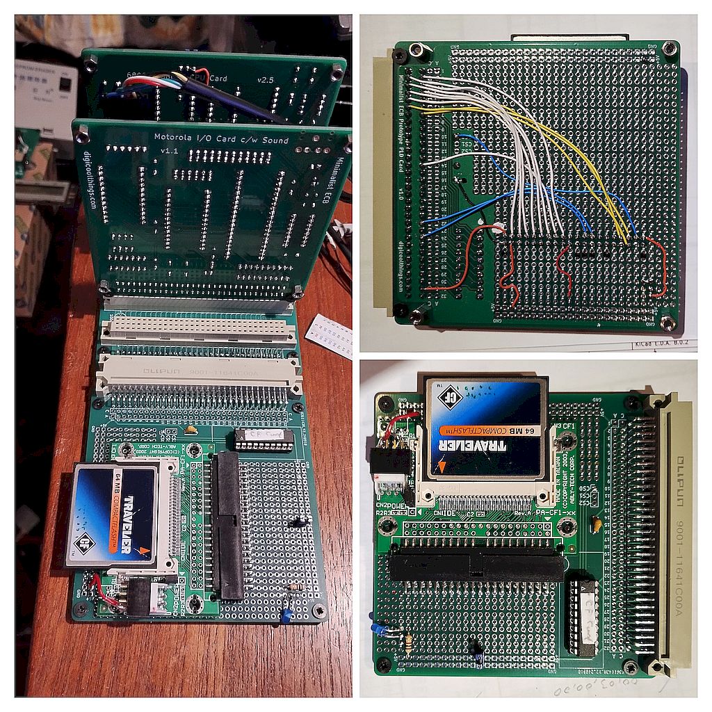
Here is the next step in my MECB journey, its an 8 bit Compact Flash interface using a prototype board and IDE CF adaptor interface. There is really nothing much to it, just some control signals, the data bus, and 3 addrerss lines. I found a suitable software to exercise it here: https://github.com/valgamaa/6809-SBC it has a menu driven interface to read the CF ID and read and write sectors etc.

Image

Code: Select all

MECB CF_Test4

>?
? - List the commands available.
B - Load the CF Card buffer with following 256 hex values.
D - Display the RAM buffer contents.
F - Fill CF Card buffer with a constant.
I - Initialise the CF Card.
L - Set the LBA address.
r - Read a data block from theCF Card.
R - Read a Flex sector from theCF Card.
w - Write a data block to the CF Card.
W - Write a Flex sector to the CF Card.
v - Verify the data block written to the CF Card.
V - Verify the Flex sector written to the CF Card.
P - Print the properties of the CF Card.
S - Set the current Flex sector.
T - Set the current Flex track.
Q - Exit this application & return to the monitor.

>I
MECB CF_Test4

>P
    Model No.: PQI ATA                                 
Firmware Rev.: 01/10/18
   Serial No.: Y011024             
    LBA Size : 00 01 00 00 

>R
MECB CF_Test4

>D
                                      
0400 18 00 11 8E 80 CD 4E 80 CD 5B 80 01 FC 00 CD FD  ......N..[......
0410 FF 20 74 CD 5B 80 45 0E 41 11 00 00 21 03 00 CD  . t.[.E.A...!...
0420 FD FF 20 63 CD 5B 80 0E 42 11 00 D0 2E 16 CD FD  .. c.[..B.......
0430 FF 20 54 CD 5B 80 11 98 80 CD 4E 80 50 1E 00 C3  . T.[.....N.P...
0440 00 E6 C5 D5 01 12 00 5F CD FD FF D1 C1 C9 C5 E5  ......._........
0450 01 15 00 2E 00 CD FD FF E1 C1 C9 3E 2E 18 E3 F5  ...........>....
0460 D5 CD 6F 80 7A CD 42 80 7B CD 42 80 D1 F1 C9 57  ..o.z.B.{.B....W
0470 CD 7E 80 5F 7A 07 07 07 07 CD 7E 80 57 C9 E6 0F  .~._z.....~.W...
                                      
0480 C6 90 27 CE 40 27 C9 11 9B 80 CD 4E 80 76 0D 0A  ..'.@'.....N.v..
0490 4C 6F 61 64 69 6E 67 00 0D 0A 00 20 52 65 61 64  Loading.... Read
04A0 20 45 72 72 6F 72 21 00 FF FF FF FF FF FF FF FF   Error!.........
04B0 FF FF FF FF FF FF FF FF FF FF FF FF FF FF FF FF  ................
04C0 FF FF FF FF FF FF FF FF FF FF FF FF FF FF FF FF  ................
04D0 FF FF FF FF FF FF FF FF FF FF FF FF FF FF FF FF  ................
04E0 FF FF FF FF FF FF FF FF FF FF FF FF FF FF FF FF  ................
04F0 FF FF FF FF FF FF FF FF FF FF FF FF FF FF FF FF  ................
                                      
0500 FF FF FF FF FF FF FF FF FF FF FF FF FF FF FF FF  ................
0510 FF FF FF FF FF FF FF FF FF FF FF FF FF FF FF FF  ................
0520 FF FF FF FF FF FF FF FF FF FF FF FF FF FF FF FF  ................
0530 FF FF FF FF FF FF FF FF FF FF FF FF FF FF FF FF  ................
0540 FF FF FF FF FF FF FF FF FF FF FF FF FF FF FF FF  ................
0550 FF FF FF FF FF FF FF FF FF FF FF FF FF FF FF FF  ................
0560 FF FF FF FF FF FF FF FF FF FF FF FF FF FF FF FF  ................
0570 FF FF FF FF FF FF FF FF FF FF FF FF FF FF FF FF  ................
                                      
0580 FF FF FF FF FF FF FF FF FF FF FF FF FF FF FF FF  ................
0590 FF FF FF FF FF FF FF FF FF FF FF FF FF FF FF FF  ................
05A0 FF FF FF FF FF FF FF FF FF FF FF FF FF FF FF FF  ................
05B0 FF FF FF FF FF FF FF FF FF FF FF FF FF FF 00 00  ................
05C0 00 00 00 00 00 00 00 00 00 00 00 00 00 00 00 00  ................
05D0 00 00 00 00 00 00 00 00 00 00 00 00 00 00 00 00  ................
05E0 00 00 00 00 00 00 00 00 00 00 00 00 00 00 00 00  ................
05F0 00 00 00 00 00 00 00 00 00 00 00 00 00 00 55 AA  ..............U.

Fortunately this is written to operate with Assis09 (albeit a modified version) but near enough to work on MECB with a couple of edits.

I've configured a Forth to work on the MECB and should soon have it working with Disk I/O with a bit of luck.
The same design has an I2C interface using a Philips PCF8584, this looks like a good way to implement it rather than bitbang which I was thinking of trying.

Best regards, David.
User avatar
djrm
Posts: 71
Joined: Wed Aug 21, 2024 9:40 pm
Location: Rillington / UK
Contact:

Re: 6809 Angel

Post by djrm »

This version of Forth includes a bare metal CF interface and was very easy to adapt for the MECB, It gave me an opportunity to test my 63C09 chip. A small hardware change was needed to connect the ACIA interrupt to the FIRQ CPU pin and then after adjusting some address decoding constants in the source it all 'just worked' The distribution comes with a CF image containing lots of examples too. I'm delighted with the outcome. https://github.com/frenchie68/Z79Forth David.

Code: Select all

nb 
\ Sample LED demo.                                              
: led-select ( ledno -- )                                       
  1 SWAP LSHIFT INVERT $c400 C! 100 MS ;                        
: led-demo ( -- )                                               
  8 0 DO I led-select LOOP                                      
  0 6 DO I led-select -1 +LOOP                                  
  BEGIN                                                         
    8 1 DO I led-select LOOP                                    
    0 6 DO I led-select -1 +LOOP                                
  AGAIN ;                                                       


                                                                 ok

                       The Game of Life
In memory of John Horton Conway 26 Dec 1937 - 11 Apr 2020

  0            *     
  1           * *    
  2    **    *  *    
  3    **     **     
  4                  
  5                  
  6               ** 
  7               ** 
  8                  
  9       *** ***    
 10      * * *   **  
 11      * *   *  *  
 12     *         *  
 13      *      **   
 14      *           
 15        ***          Generation = 34 
User avatar
djrm
Posts: 71
Joined: Wed Aug 21, 2024 9:40 pm
Location: Rillington / UK
Contact:

Re: 6809 Angel

Post by djrm »

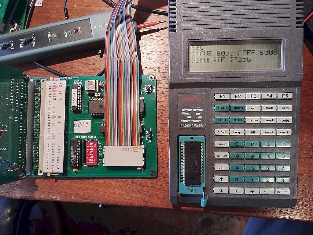
Some years ago I rescued this Dataman S3 eprom programmer / emulator although I have never used it as an emulator until today.
Here is is connected to my MECB 6309 CPU board.
Image

I was using it to incorporate the rtc-72421 clock reading primitives into the Z79 Forth system. Seems ok but a bit slow. When some new flash chips arrive I can use it to debug in circuit flash writing perhaps.

Here is the initial crude clock display word and result

Code: Select all

: 2digitsout ( n -- ) S>D <# # # #> TYPE ;

18 string-table month-table
" Jan"   " Feb"   " Mar"   " Apr"   " May"   " Jun"
" Jul"   " Aug"   " Sep"   " 10" " 11" " 12" " 13" " 14" " 15" 
" Oct"   " Nov"   " Dec"

: wdate ( -- )  
WARNING: wdate is being redefined

  CR WTC@ 
  base @ >r 
  hex swap rot 
  2digitsout [CHAR] : EMIT 
  2digitsout [CHAR] : EMIT 
  2digitsout [CHAR] : EMIT 
 
  BL EMIT   
  swap rot 
  $20 2digitsout 2digitsout 
  BL EMIT   
  month-table 
  2digitsout  
  r> base ! 
  ;  ok

wdate 
22:31:47: 2024 Oct 08 ok

Post Reply