
I’ve now added a flexible Banked Memory Expansion Card to the MECB Card range, enabling any of the existing (or future), 8-bit CPU Cards to be expanded with a Banked Memory solution.
This allows expanding your 6809, 6309, 6802, 6502, or even a Z80 CPU card (or any other future 8-bit CPU Card), to have up to 3.5MB of addressable RAM memory available!
In the linked video (below), I introduce the background, go through the design, schematic and PCB layout, and then take you through assembling one. I then write a couple of 6809 Assembly Code examples of the Banked Memory Card use.
Introduction
I’ve spent far too long, contemplating a Banked Memory solution for MECB.
Basically, I had been distracted, caught up with thinking solely of a Z80 based memory banking (or paging), solution. Solely with the thought of implementing a Z80 based operating system.
However, in a moment of reflection, I realised that this wasn’t staying true to my original intent for MECB.
As a reminder, my Minimalist ECB platform is intended (first and foremost), to be a platform for experimenting with the different original 8-bit devices.
It is also intended, to be a platform where you can mix-and-match different CPU Cards with different Peripheral Cards (using it’s bus backplane), to build whatever system you might like to put together.
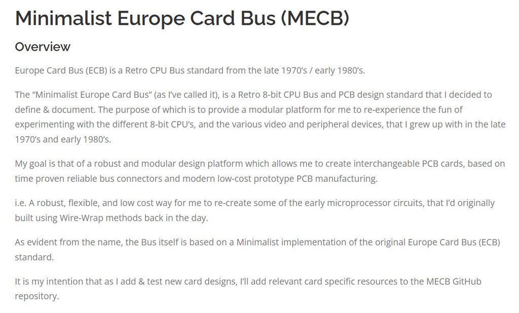
With this in mind, it was obvious that, in terms of a Z80 CPU Card, I should instead be creating a simple Z80 CPU Card, basically along the same lines as my existing 6809, 6802, and 6502 8-bit CPU Cards.
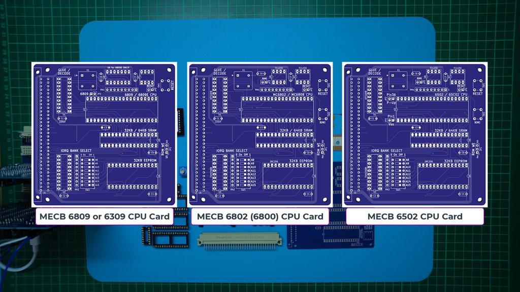
This would allow the use of a Z80 monitor ROM, for direct experimentation with the Z80 CPU itself, with no need for the added complexity of a larger, banked, memory system.
So, this would address the MECB intent of a Z80 CPU Card to experiment with, to allow getting familiar with the Z80 Instruction Set Architecture (ISA).
A Banked Memory Solution for MECB
Separate to this, is then having a Banked Memory solution, ideally, which you can mix-and-match with your choice of 8-bit CPU.
So, with this in mind, I now present what I’ve come up with, for a generalised MECB Banked Memory Expansion Card.
Firstly, each card provides up to 1MB of memory, organised into four 16KB Banks.
Theoretically, you could add 3 of these Cards to your system, to provide 3MB of banked RAM memory.
In addition to 1MB of RAM, the Card holds a 16KB bank of ROM, with that ROM Bank being manually (Rotary Switch), selected from 16 possible 16KB ROM banks (so, that’s 256KB of ROM in total).
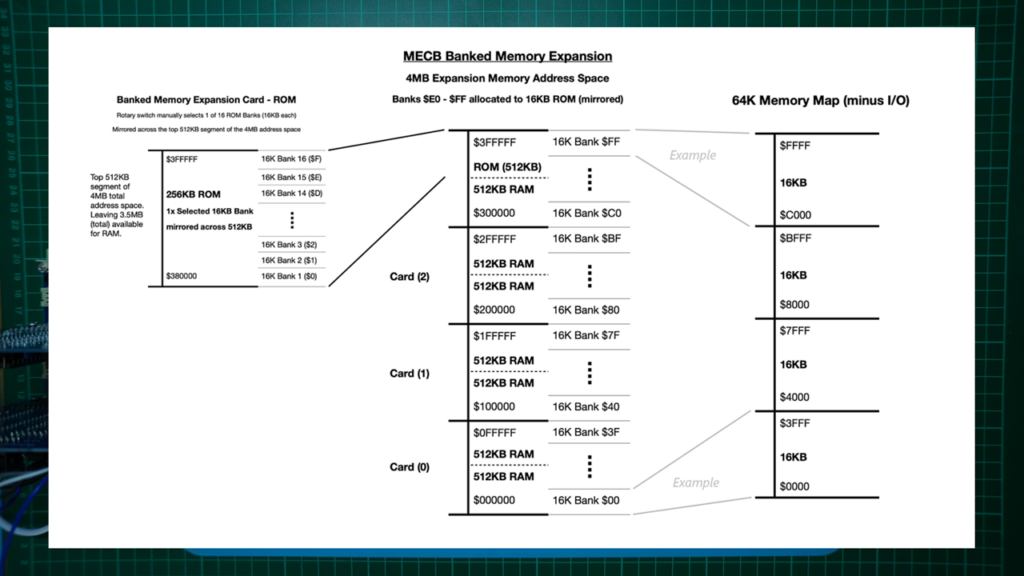
Only having 16KB of ROM available, and focussing on program selected Banks of RAM, makes the most sense, as most banked memory solutions involve the operating code being loaded into RAM, from mass storage.
Therefore, the actual requirement for ROM is generally only for boot-loading the system.
For this purpose, 16KB is more than enough for either boot-loading an operating system (from a mass storage device), or, for simply boot-loading a smaller ROM resident monitor, or other application.
By providing 16 switched ROM Banks, this also supports the MECB intent of experimentation and mix-and-match.
You could simply pre-program different ROM boot-loaders, even for different CPU’s, all then available at the twist of a rotary switch! No re-programming or ROM swapping is necessary, to swap to a different CPU Card, or, to a different operating system / monitor for the same CPU Card.
The approach is that upon hardware reset, the 16KB ROM bank, by default, is mirrored 4 times across the 64K memory space. This supports processors that boot from a bottom of memory reset vector (like the Z80), or from a top of memory reset vector (like the 6809 etc.).
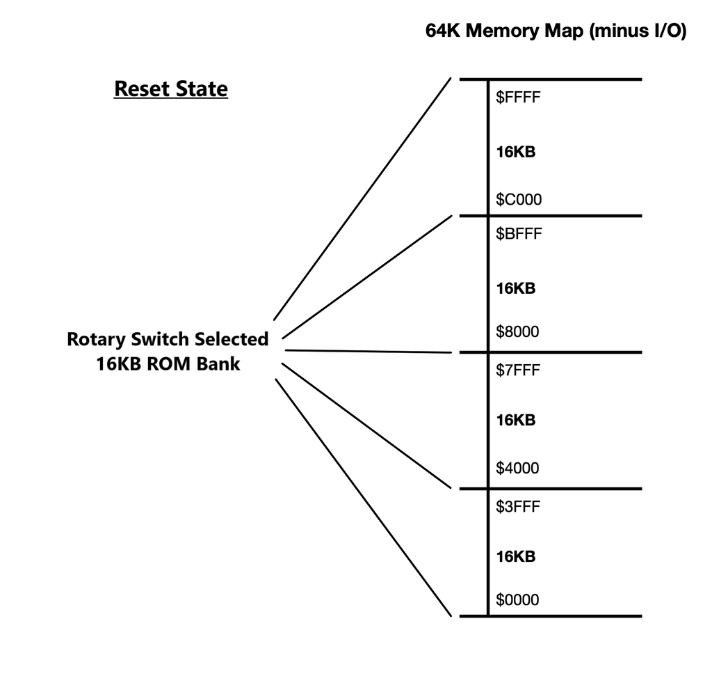
You then just need a small boot-loader routine, which arranges your memory banks how you want, and then turns on the memory bank selection system, giving access to the RAM.
Combined with the standard MECB PLD based glue logic, you can easily define Bank Control register addressing, and also define if this is a first, second, or third Banked Memory Expansion Card in your system.
Overall, a very flexible solution, which perfectly fits in with the intent of MECB.
Banked Memory Card Schematic
So, let’s take a look at the schematic.
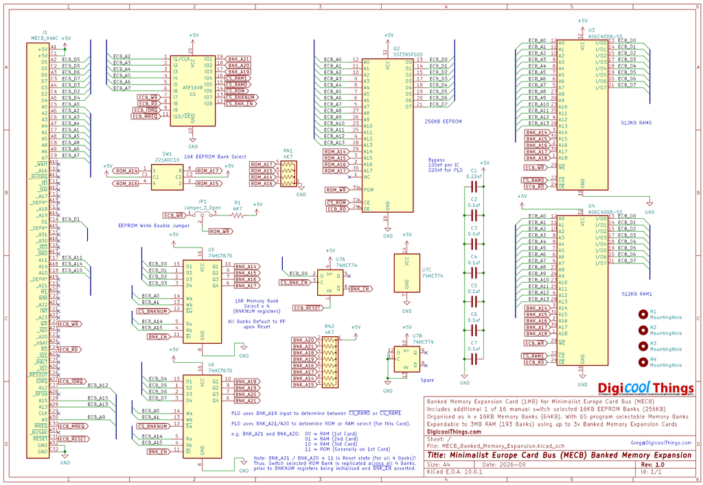
Firstly, we have one or two 512KB SRAM chips, for a total of 1MB of available RAM memory (per Card).
Secondly, we have a single 256KB ROM chip, for a total of 256KB of available ROM memory.
As you’ll note, the 14 lowest address lines A0 – A13 of the various memory chips come directly from the bus, which therefore directly addresses a 16K page (or Bank) of memory.
The upper address lines of each RAM memory chip, however, comes from the Banked Memory Selection logic. This entails four 8-bit registers which define the four 16K memory banks which will make up our 64K 8-bit CPU addressing space.
This is achieved by the remaining two CPU bus address lines, A14 & A15, selecting one of the four 8 bit registers to provide the upper 8 address lines for each of the four 16K segments of the 64K address space.
With 8 bit registers, combined with the 14 lowest address lines, we have a total of 22 address lines, A0 – A21, giving an overall addressable space of 4MB, from which to select each of the four possible concurrent 16KB memory banks.
The upper address lines of the ROM memory chip, however, instead come from a 1-of-16 Rotary Coded selection switch. This provides the manual selection of 1-of-16 power-on boot-loader ROM banks.
In addition to the four 8-bit registers, for selecting four 16K memory banks from a total 4MB address space, we also have a single bit register (or flip-flop), for enabling or disabling the memory banking logic.
Upon system reset, this 1 bit enabling register is reset to the disabled state. This results in all of the 8 bit bank select register outputs being in a hi-impedance state (Tri-state). In this case, the pull-up resistor bank initially sets all four banks to be $FF. Effectively defaulting the memory card to the top 16K bank of our 4MB total memory address space, as being the selected Bank for all 4 of the possible 16KB banks.
For providing the Chip Select output for each of our three onboard memory chips, and for the Chip Select of our memory bank registers and single bit enable register, we use our PLD glue logic.
Firstly, we have six low-order MECB bus Address lines A2 – A7, to allow defining the I/O address allocation of our control logic.
Secondly, we have the three high-order Memory Card address lines A19 – A21, which enables our PLD to split our 4M addressing space into 8 segments of 512K each.
The top 512K segment (the eighth segment), we allocate to the ROM, to ensure it is selected by default after a hardware reset. i.e. Segment 8, or binary 0b111 (for address lines A19 – A21).
This actually leaves seven 512K segments available for RAM selection, or a total of 3.5MB of RAM.
However, I have no reason to believe that anyone would actually need 3.5MB of RAM for their retro 8-bit system.
Therefore, I’ve just thought of the RAM being potentially expandable to 3MB, across three Cards (instead of the potential of 3.5MB across four Cards).
I suspect it is more likely that 1MB on a single Card is more than enough, perhaps going to a two Card 2MB setup, if really needed.
On this basis I plan to offer pre-programmed PLD chips only for either a first (Card 0) or a second (Card 1) Memory Expansion Card. But, I will be sure to include options in the PLD source code for enabling up to four Cards.
Banked Memory Card PCB Layout
So, let’s now look at the PCB layout.
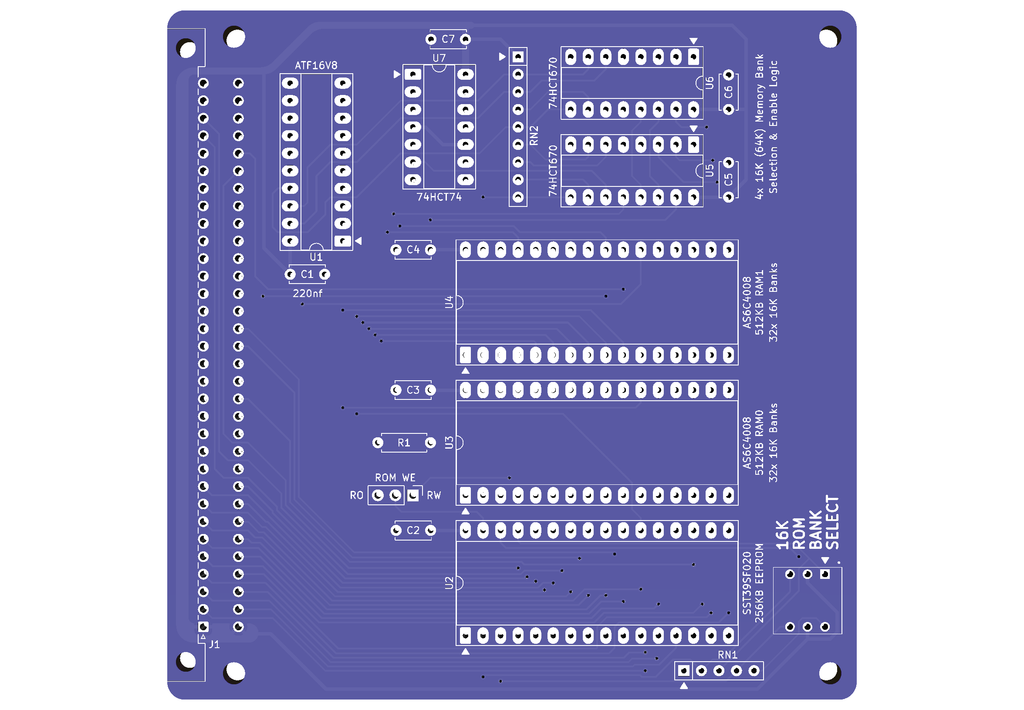
As you can see, the layout is relatively clean and organised.
Aside from the 3 memory chips, we have a section for the Bank Selection Logic, and we have a ROM bank selection rotary switch, which is positioned at the exposed edge of the card.
Banked Memory Card Assembly
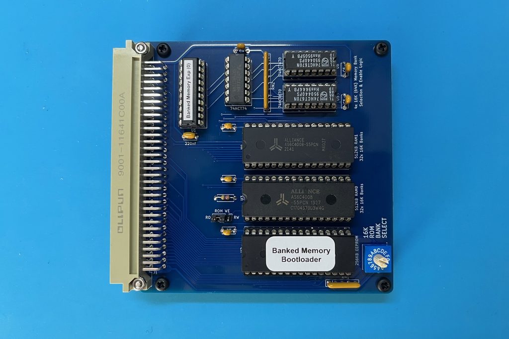
So, it’s time to get the first one assembled.
As usual, I start with the lowest profile components, and progressively work up to the highest profile components last (which, in this case, is the Rotary Switch).
For a full walk-through of the assembly, be sure to watch the linked video.
Glue Logic PLD Code
Okay, lets take a look at the PLD source code.
Firstly I now use the new WinCUPL II which is available as a free download from Microchip, and runs perfectly on Windows 11, unlike the original WinCUPL.
For a visual code walk-through, be sure to watch the linked video.
Also, the full code can be found on the MECB github repository.
In summary, first I have the standard header, and then the input and output pin declarations.
Next I have the logic equation for the four Bank Register’s chip select, which occupies the I/O addresses $78 – $7B Followed by the Bank Enable chip select register, which is located at $7C mirrored across 4 locations to $7F
Of note is that both of these chip selects are write-only, so only asserted during an ECB write.
Next, I have the ROM chip select, which encompasses the top 512K segment of the 4M addressing space.
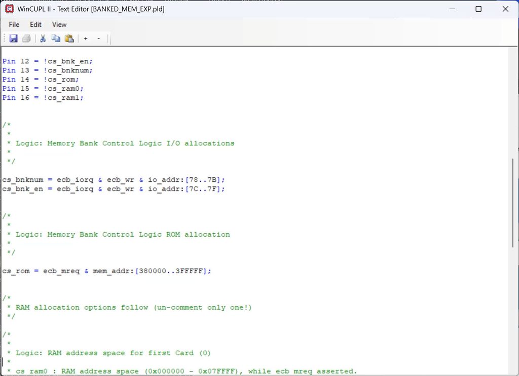
Finally we have a pair of RAM chip selects. These are setup for each of 4 possible Banked Memory Expansion Cards, that you could have in a single system. All are currently commented out in the code, except for the first card RAM chip selects for the bottom two 512K segments of our 4M addressing space.
Boot-loader ROM
So, let’s now move onto our ROM code.
My thought for testing the Banked Memory Expansion Card is to use my 6809 CPU Card to create a customised ASSIST09 monitor ROM, which has been extended with a “Bootloader”, to initialise the system for the Banked Memory.
At reset, the 64K memory space is initially filled with 4x 16K images of the ROM code. So, no RAM is available for a stack or any storage.
Therefore, the first step would logically be to set the 4 memory banks for a mix of RAM with the ROM bank left where the reset code is currently running.
In the case of the 6809, the reset vectors are stored at the top of memory, so the running ROM code is likely within the top bank. We could therefore just set the initial four bank registers as three Banks of RAM, 0, 1, 2, and our ROM bank $FF. Then we can enable the Memory Banking, and pass control to ASSIST09.
This would give us the simplest initial availability of RAM, with a straight-forward 48K RAM + 16K ROM memory map. Basically, 3 selected RAM banks and the ROM bank.
So, for this we’ll also leave our CPU card setup for a $C0xx I/O Bank, and use our 48K / 16K configured ASSIST09 source code.
Let’s have a look at that.
Boot-loader ROM Code – A Simple Example
Okay, so to keep things simple, I’ve just copied the ASSIST09 source, and I’ve simply modified it’s reset vector to now point at our new boot loader code (BOOTLD).
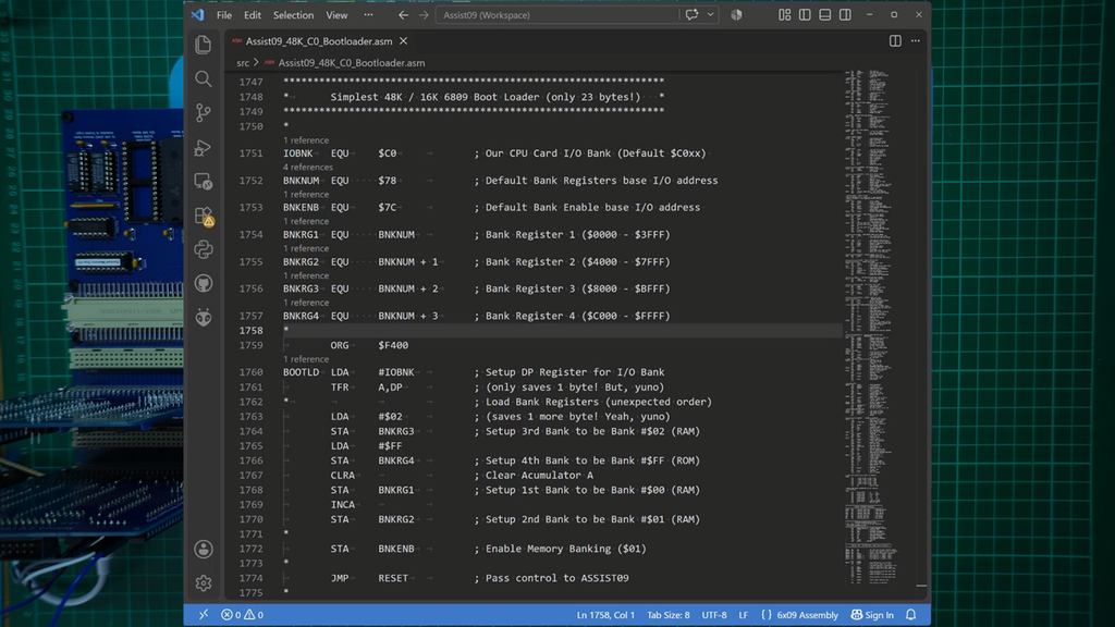
For the boot loader, I first write out the 4 required banks to the 4 bank registers.
These are Banks 0, 1, 2, and $FF (for our ROM bank which our reset code will be running in).
Now, a couple of things to remember.
Firstly, following reset, we have no RAM available, as the entire 64K memory space is, at this time, simply 4 images of our switch selected 16KB ROM Bank.
Therefore, we initially have no storage or stack available. So, we have no need to initialise the stack pointer at this boot loader stage, and we also don’t want to call any subroutines, or, do anything else that will result in using the stack.
Secondly, we should keep in mind that the memory bank selection registers, and also the bank enable register, are write only! Therefore, we cannot read the current values!
So, I simply start by writing out the four required memory bank register values.
Then, I write a ‘1’ to the bank enable address, to enable the memory banking.
Now, as you’ll note from my comments (in the code listing), I’ve decided to use the direct page register and to also use an unexpected sequence for writing our 4 bank registers.
This is all in the interests of saving a couple of bytes, and getting our “minimal” boot loader to be only 23 bytes.
Now, I’m usually more in favour of keeping code as simple and as readable as possible, but on this occasion, I thought I’d just go for a smaller code size.
At this time we should now have a 48K RAM + 16K ROM memory map, so I can now simply jump to the original ASSIST09 reset vector address, to pass control to ASSIST09.
This is the simplest boot loader I can put together for an initial test.
So, this is currently assembled and loaded into the first 16K bank of the ROM, which I earlier inserted into our Banked Memory Card.
So, with the memory chips already removed from my 6809 CPU Card, and the CPU Card I/O Bank select switch set to $C0xx, we are ready to do our first test.
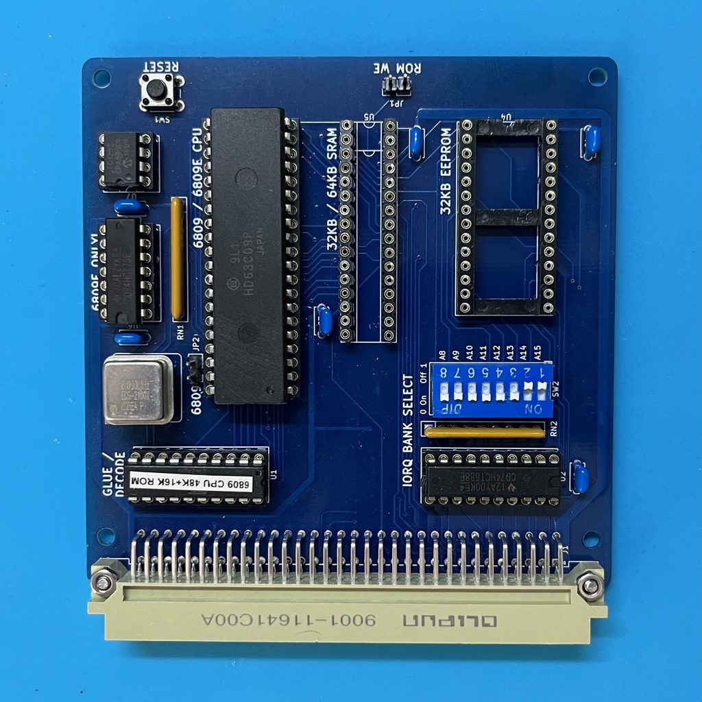
Okay, let’s power on, and see if we have a working solution.
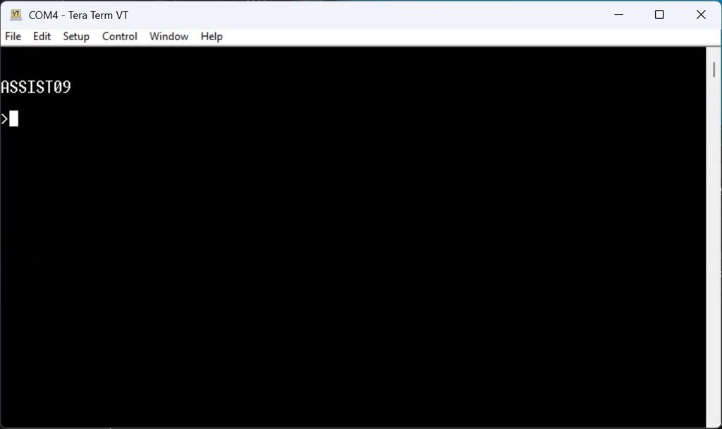
Looking good. We have our ASSIST09 prompt, so we know ASSIST09 is up and running with it’s RAM workspace.
Now, knowing that ASSIST09 positions it’s RAM workspace, and stack, at the top of RAM, we are free to play with the lower two RAM Banks.
So, lets start off by writing $55 into the first byte of RAM at address $0000
And view it again, for confirmation.
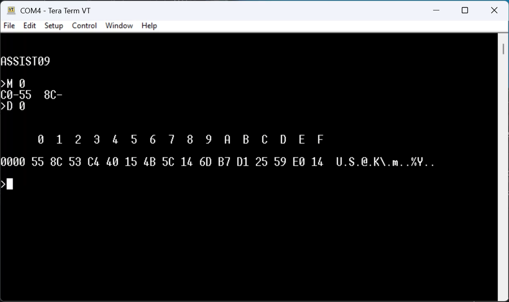
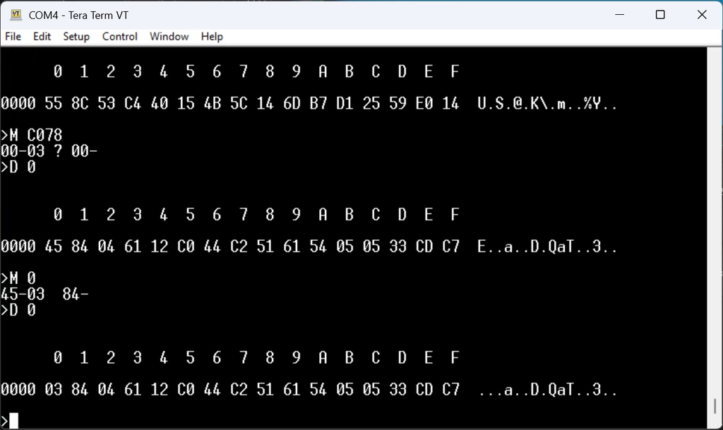
Now if I write $03 to the first Bank register, we should have changed the lower 16KB of RAM to now be bank 3, instead of our original Bank 0.
Note that as the Bank Registers are write only, we can write a value to the register, but ASSIST09 issues a question mark error, as it’s not able to read back the written value for verification.
So, let’s take a look at memory address $0000 again.
And we can see our $55 byte has gone.
So, let’s now store $03 to address $0000.
And, view it again for confirmation.
Okay, now let’s write bank number $00 to the first Bank Register, so we should change the lower 16KB of RAM back to the original Bank 0.
Let’s take a look at memory address $0000 again.
And, we can see that our $55 byte is back again. Not the $03 byte we wrote into the first byte of Bank 3.
Just to be doubly sure, I’ll again switch to Bank 3, by writing $03 into the first Bank register.
And, take another look at memory address $0000 again.
Yes, we have our $03 byte back again, that we earlier stored in Bank 3.
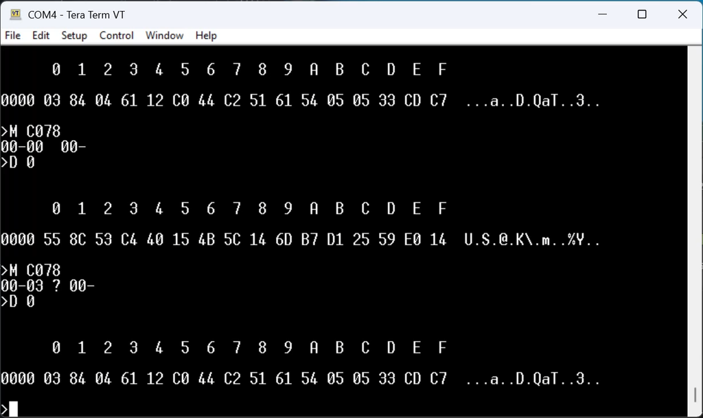
So, all is looking great! It looks like we have a fully functioning Memory Banking system.
Boot-loader ROM Code – A more Advanced Example
So, next, let’s take a look at a more advanced boot loader.
My preferred 6809 system, uses an expanded 56K RAM + 8K ROM memory map.
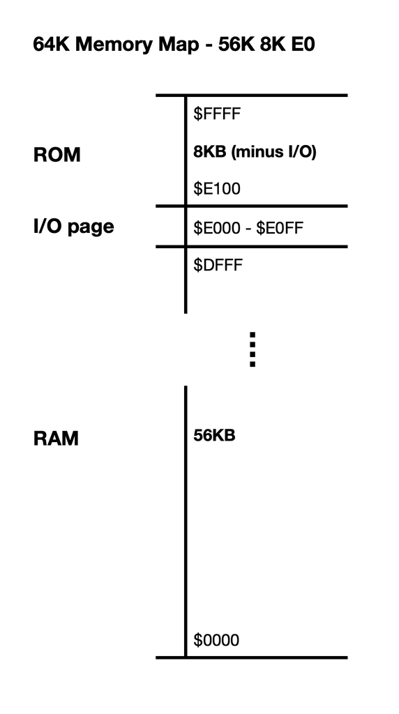
To achieve this, we would instead take the option of copying the top 8K of the 16K ROM image into a RAM bank, and then swapping out the monitor ROM bank for this RAM bank.
Remembering also that ASSIST09 is only 2K of code, so we have plenty of space for a boot-loader.
In this regard, it would even be feasible to implement a 60K RAM + 4K ROM memory map, with the I/O Bank relocated to $F0xx.
But, for now, lets just focus on our usual 56K + 8K memory map, with the I/O Bank at $E0xx.
Ideally (although not essential), it would also be nice to perform a non-destructive RAM test, to enable us to report on the total Banked Memory that is available.
This would be quite useful, from the perspective that we might have only 512KB RAM installed on our Banked Memory Expansion Card (for 32 banks), or, we could have the full 1MB (as 64 banks), or, we could even have a second, or third, card installed (giving 96, 128, 160, or even 192 banks of RAM).
For a non-destructive test, we could read a memory value, store back the complemented (inverted) value, and read it back again to verify that we have RAM. Finally, restoring the original / non-inverted value.
This would enable the total number of available RAM “Banks” to be accumulated as a 8 bit unsigned integer (byte), as a 0 to 192 count of detected 16K RAM Banks. Or, perhaps even 224 banks of RAM, with a 4 card system. Yeah, I know, that would be crazy!
With a single fully populated (1MB), Banked Memory Expansion Card we should have 64 banks, which is 1,048,576 bytes in total.
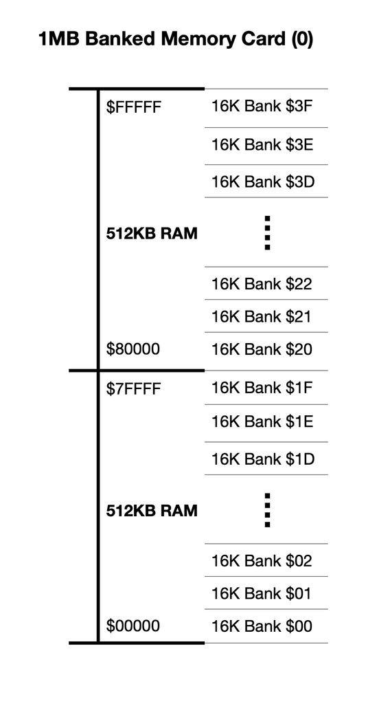
So, lets take a look at the code I’ve put together for this.
For this you can view the walk-thorough in the linked video, and/or, obtain the source code from the MECB github repository.
Okay, so with this new enhanced boot loader code assembled and programmed into the second bank of the ROM, I just need to switch my CPU Card’s I/O Bank to be $E0
Then we’re ready to test. So, let’s power on, and see what we get.
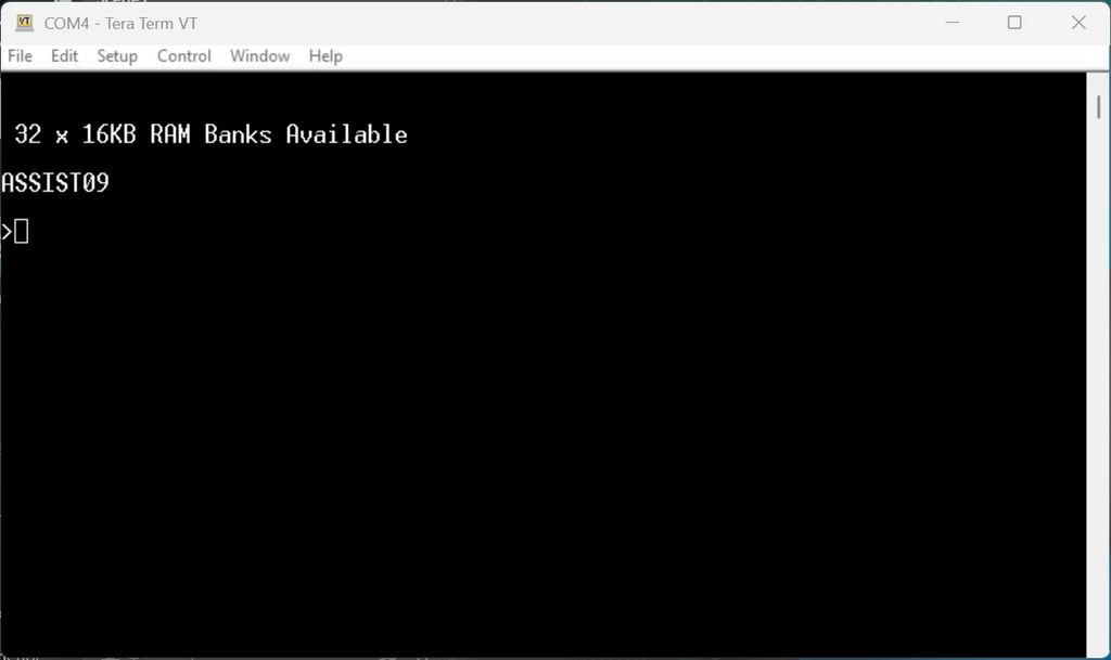
Looking good. We have the expected 32 Banks reported for our initial 512KB (single SRAM chip), loaded Banked Memory Expansion Card.
So, let’s now insert our 2nd 512KB Static RAM chip, for a full 1MB Memory Card.
And lets power on, and see what we get.
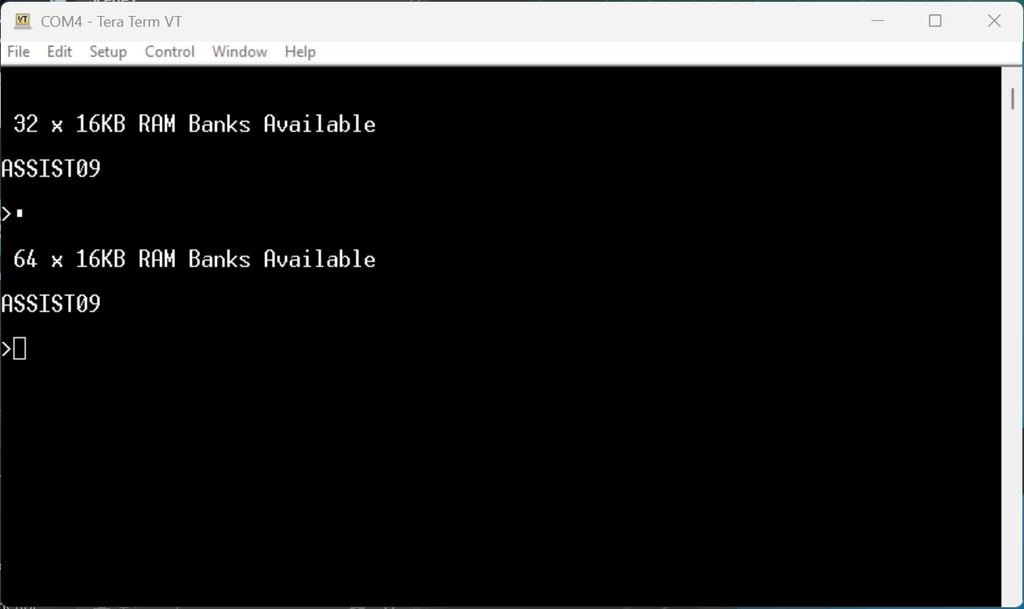
Yes, we now have 64 Banks reported, as expected.
Adding a 2nd Banked Memory Expansion Card
So, now for some fun.
I’ve assembled a second Banked Memory Expansion Card, so we can try inserting two into our system. Just to prove that using multiple cards, does work!
Here is my pre-assembled additional card.
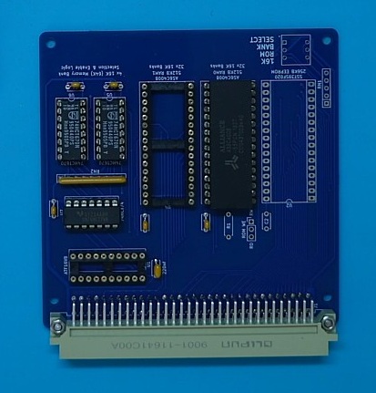
The first thing that you’ll note is that I’ve assembled the Card with all of the ROM related components left off, as (of course), we only need our ROM on our first card.
So, the only missing component to get us under way, is the PLD.
The PLD code is what differentiate the Banked memory Expansion Cards.
So, I’ll install the PLD which I’ve programmed with the second Card RAM space allocation.
Now, with just the one 512KB RAM chip installed, let’s insert it in our backplane, and power-up.
And, we have our expected 96 RAM Banks reported. Which equates to 1.5MB of RAM.
So, lastly, I’ll insert the 2nd 512K RAM chip in our 2nd Card, which gives us a full 2MB of RAM (across two Cards).
Let’s power-up.
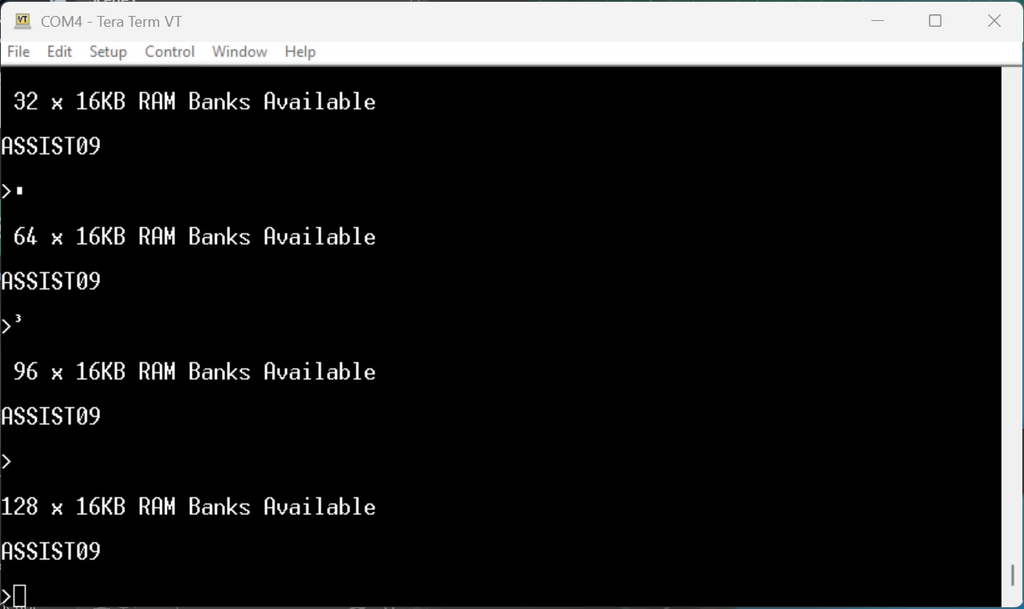
So, we have the expected 128 Banks of RAM reported.
This completes our initial MECB Banked Memory Expansion Card test examples (for use with a 6809 or 6309 system).
Next Step – Mass Storage
The next step will be to add a mass storage device, so that we are not restricted to only boot-loading code that can fit into 16K of ROM.
For this I have already designed a couple of new MECB Mass Storage Card options, which I plan to test next.
Available in my Online Store
In the meantime, you can find the MECB Banked Memory Expansion Card on my online store.
As usual, I’ve listed as PCB only, with optional packs to make up a full kitset.
Here are the optional packs.
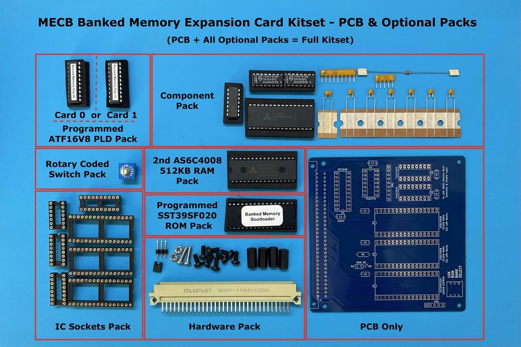
The Programmed SST39SF020 ROM will initially contain the two 6809 boot loader examples, but I may also add more banks to the pre-programmed ROM, for different CPUs and for added functionality, as time permits.
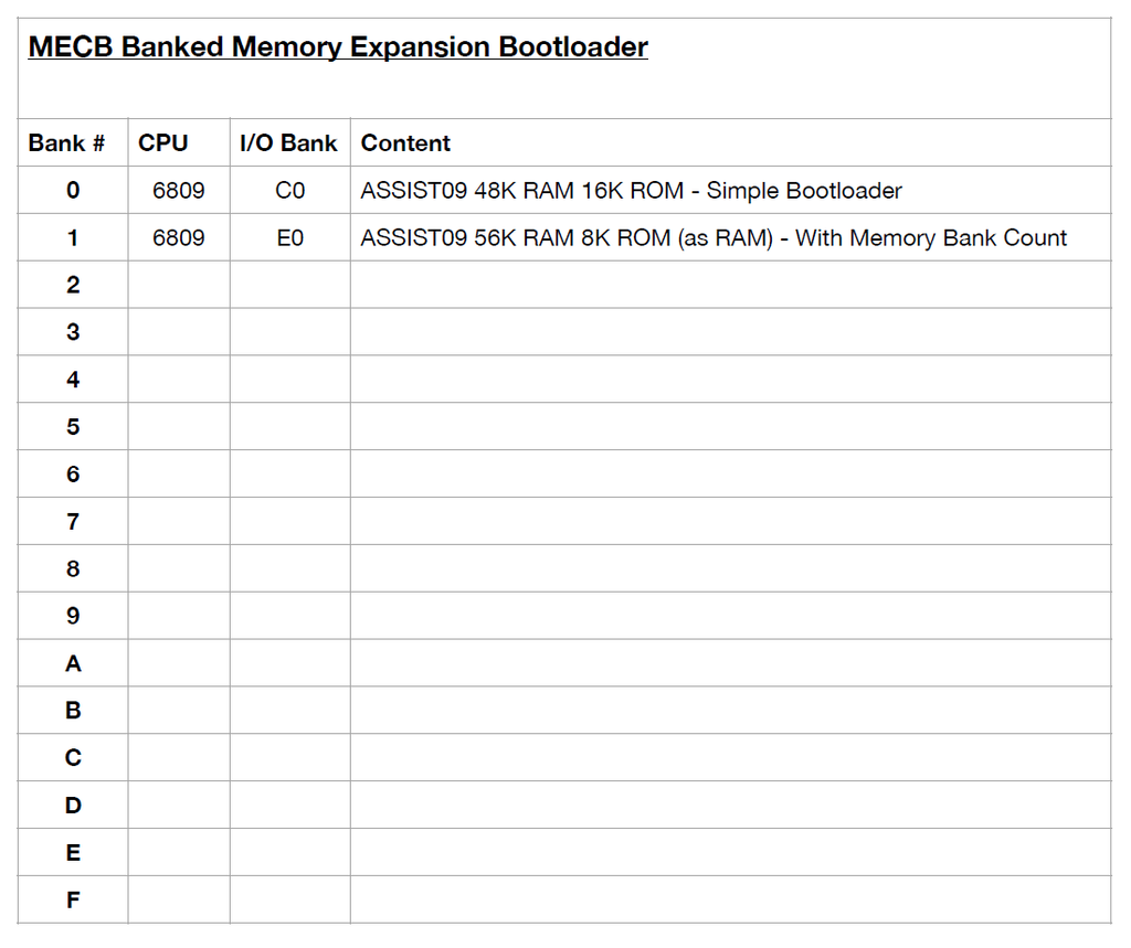
As usual, resources can be found on the MECB Github.
I look forward to hearing what systems you put together, using the extra available memory space provided by the MECB Banked Memory Expansion cards.
Most importantly, Have Fun!