
After designing my 6809 CPU Card, the next CPU on my wish list was the 6502.
Join me, as I walk-through the design, then I assemble and test my first 6502 Card.
After building homebuilt systems in the early 1980’s, based on the 8-bit Motorola 6800 and 6809 CPU’s, my first introduction to the 6502 was when I bought my first Commodore 64.
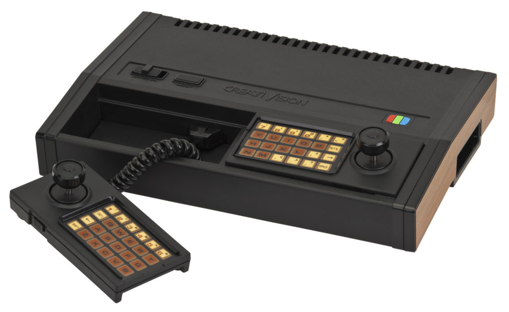
My interest in making a 6502 CPU Card, was also due to a desire to replicate the 80’s CreatiVision gaming console, on an MECB system.
The CreatiVision was, of course, also based on the 6502.
Now, I’m a bit embarrassed it has taken me so long to make this post / video. As this particular 6502 CPU Card design was actually completed at the end of last year (2023). On the Schematic, that I’ll show shortly, you’ll see it is dated November 2023.
The prototype PCB’s were received in December 2023.
But, unfortunately, the beginning of 2024 I was kept busy with flood recovery projects around the house, so the 6502 CPU Card PCBs ended up on my shelf, awaiting my attention.
So, let’s dive in, by first taking a look at the schematic.
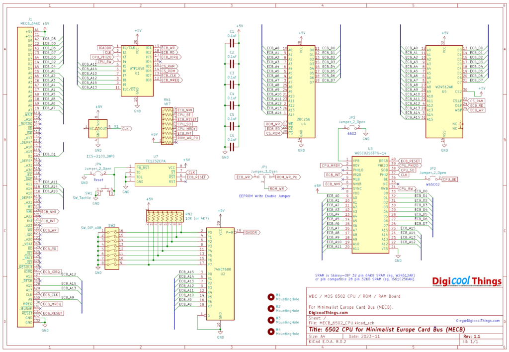
As you can see, this schematic was designed in November 2023.
You’ll perhaps also note the similarities with the final version of the MECB 6809 CPU Card.
The 6502 CPU Card has been based on the earlier 6809 CPU Card design, which certainly makes sense, given the similarities between them.
For the 6502 CPU Card I wanted to also ensure I was supporting both the original MOS 6502 CPU chip, as well as the currently still in-production Western Design Center W65C02 version.
As it turns out there are only a couple of pin differences that are relevant to us between these two devices.
The first is pin 1, which is a second Vss (or GND) connection on the original MOS 6502, but is a Vector Pull output on the newer W65C02.
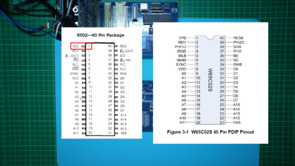
Due to this, we need a Jumper to connect pin 1 to GND, only when using the MOS 6502.
Secondly, we have pin 36 which is a No-Connect (NC) pin on the original MOS 6502, but is used as a Bus Enable pin on the W65C02.
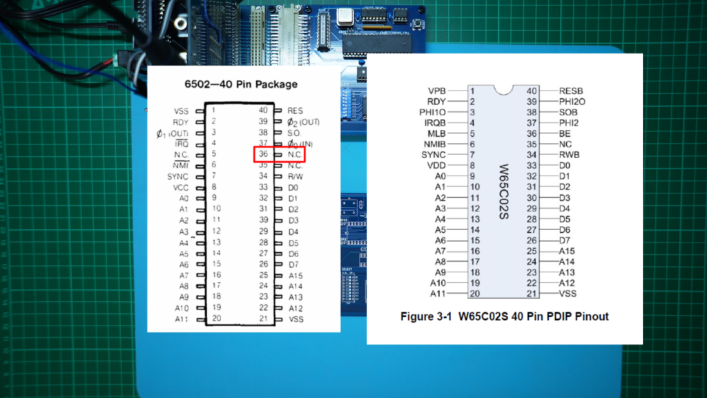
Bus Enable must be pulled high for the bus’s to be active on a W65C02.
To honour the No-Connect pin on the original 6502 (that shouldn’t be connected), we also need a Jumper to pull pin 36 high, only when using the WDC W65C02.
The rest of the schematic virtually duplicates what we’ve already implemented, and tested, for the 6809 CPU Card.
This includes our TC1232 Reset chip, our I/O Request bank select, and the use of our standard ATF16V8 PLD for the glue logic.
We also have the same 32KB or 64KB fast SRAM chip, and our 32KB AT28C256 EEPROM chip.
So, we have the same memory map flexibility that we implemented earlier on the 6809 CPU Card, and also as per the flexible design intention of MECB.
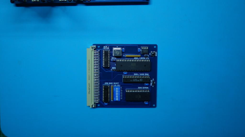
Okay, so here is one of the first prototype PCBs received in December last year.
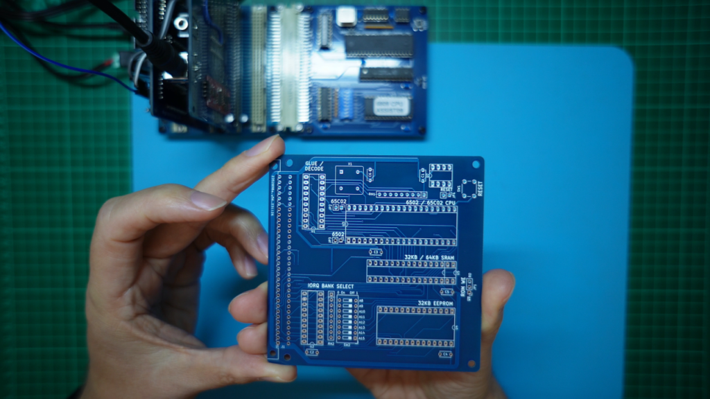
Now seems like a good time to assemble our first one, ready for testing!
With our first PCB assembled, it’s time to populate the IC’s.
First I inserted the 74HCT688 8 bit Comparator, for the IO Request bank select. Then, our TC1232 Reset IC. Next, a 64K Static RAM chip.
For our first test I just use a 1MHz crystal oscillator, so that we are starting out with a clock speed that should work for all chip variants.
For the CPU, we start by testing a brand new WDC W65C02S processor. So, I next insert the WDC CPU, and also the 65C02 jumper.
This then just leaves our PLD, for the glue logic, and a ROM.
Firstly, let’s take a look at the WinCUPL PLD source that I’ve put together for the 6502 CPU Card.
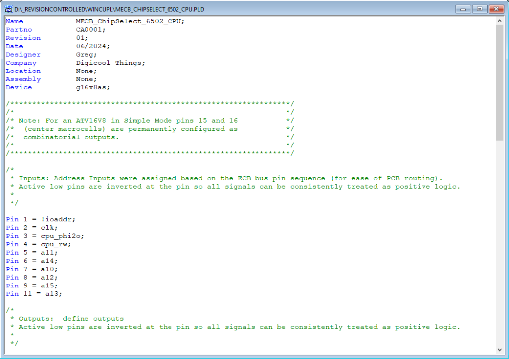
First we have the standard WinCUPL source header.
Then I declare the input pins.
Here you’ll note that I routed both the oscillator clock clk, and also the 6502’s Phase 2 output clock cpu_phi2o, to the PLD.
The reason for this is to give the choice of using either the 6502’s Phase 2 clock output, or the master oscillator clock, as the main bus and timing clock source.
This is to allow for backward compatibility, as the WDC W65C02 datasheet indicates that the Phase 1 and Phase 2 outputs should no longer be used. Instead the system clock should just be based on your main oscillator clock (i.e. the Phase 0 Input clock).
It also states that the Phase 2 Clock output was only used when the Clock input pin was crystal driven.
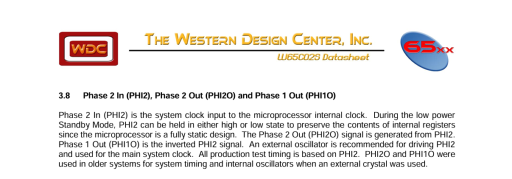
In effect the Phase 2 clock output of a 6502 is just the buffered output of the Phase 0 input.
Meaning that other than a small propagation delay, it is identical to the master clock input.
So, I’ll initially base the timing and Bus clock on the master clock input, but I’ve also allowed for using the Phase 2 output clock instead (if it turns out it’s needed).
Ok, next we have the output pin declarations.
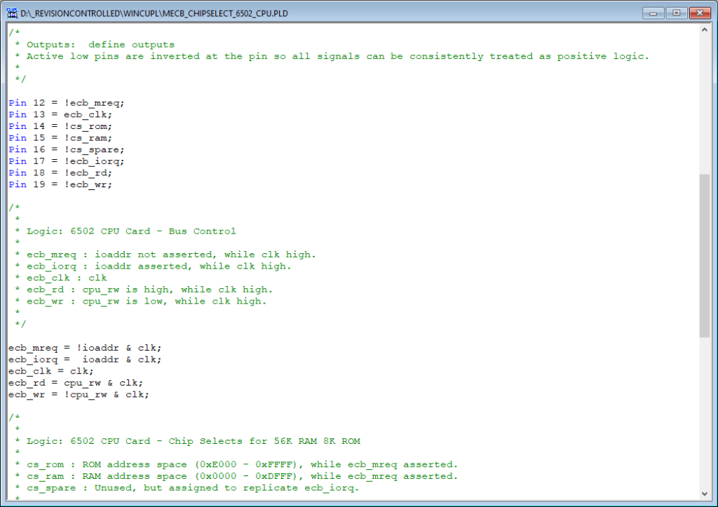
As noted in previous posts / videos, you’ll see that active low signals are inverted at the pin declarations, so that all the logic equations. which follow, can be based on positive logic, for simplicity and ease of understanding.
In other words, less prone to making logic errors!
Next, I have the logic for generating the standard Control Bus signals.
Again, note I am initially basing this on the system clock input pin clk. We could optionally change all the clk references to the cpu_phi2o signal instead, if needed.
Lastly, we have the logic for generating the Chip Select signals for our on-board RAM and ROM.
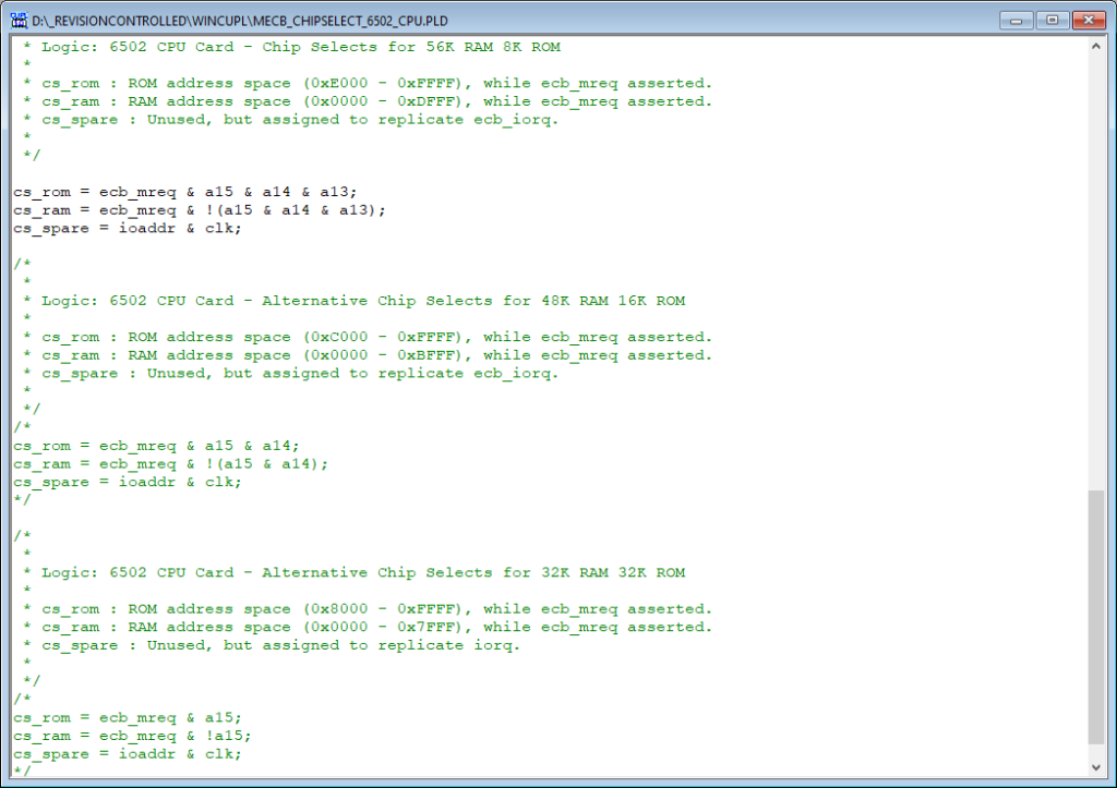
I’ve commented out options for 48K + 16K, and 32K + 32K, so they’re ready if needed. But initially I’ve gone with a full 56K RAM and 8K ROM.
With that explained, I next program an ATF16V8 PLD chip and get that inserted on the PCB.
With the PLD inserted, I also set the CPU Card’s I/O Bank Select switch to be at $E000, which effectively replaces the bottom page of the allocated ROM space.
So, we have switches 1 – 3 set to Off, and the others On, for Bank $E0.
This just leaves writing some code, to enable us to test our initial prototype MECB 6502 CPU Card.
For this, there was the option of diving into a full monitor program.
But, as we did in the old days, the best way to test a new microprocessor hardware design is to write some simple “Hello World” code, that we can load into a ROM, to test if our design is alive!
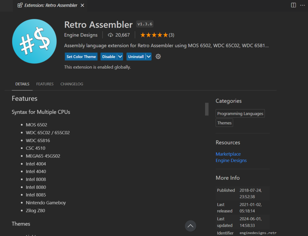
For a 6502 Assembler, I took a look at what was available as an extension for the Visual Studio Code editor, that I have been using for my 6809 Assembly code editing.
I came across the Retro Assembler plug-in that looks to be currently maintained, and also specifically supports both the original MOS 6502 and the WDC 65C02 (and others).
So, let’s take a look at my first Hello World 6502 code.
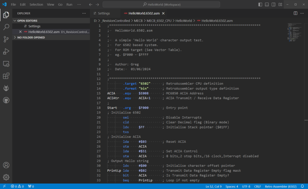
As you can see, I’ve nicely commented it, as I usually do.
First we have a couple of RetroAssembler specific directives. Firstly to ensure we are in 6502 CPU mode, and secondly to specify a .bin assembler output format (ready for programming into ROM).
Then, I declare the address of our ACIA chip, which resides on our MECB Motorola IO Card. As you’ll recall, I set the I/O bank to the $F0 page, so our ACIA will be at $E008. Or, more specifically, the ACIA Control register is at $E008, followed by the ACIA Data register at $E009.
Next we have the start of our code, where I initialise the 6502. Although not necessary, I think it’s good practice to fire-up the system by ensuring interrupts are disabled, we are in binary mode (instead of BCD), and that the Stack Pointer is initialised to the top of the stack (even though we are not using the stack here).
Next, we initialise the 6850 ACIA chip, with a master reset and then setting up the control register.
Finally, we have our main loop where we output the Hello World string that we’ve declared below.
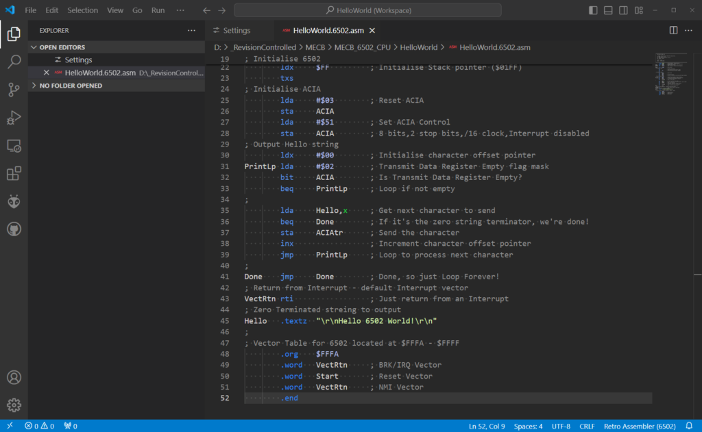
Note that the string is declared as a zero terminated string, so we can loop through outputting characters to the ACIA, every time the transmit register is empty, until we have a zero character.
Then finally, we just end in a never-ending loop (Done).
So, a pretty safe and simple little program, for testing our 6502 is alive, with a Hello 6502 World message!
Lastly, in the source, we declare our three standard 6502 vectors from $FFFA.
For the Interrupts, we just point to an immediate RTI, Return from Interrupt. And for Reset, we point to the Start label at the entry point of our Code.
So, with Retro Assembler we just need to press Ctl-Shift-B to build our .bin file.
As we originate our code at $F000, and we have the vectors declared from $FFFA to $FFFF, we have a 4KB .bin file output from our simple program.
So, next I get that programmed into a 28C256 EEPROM.
As the 28C256 is a 32K ROM, I need to load the 4KB bin file into the programmers buffer at $7000, to put it into the top 4KB of the ROM.
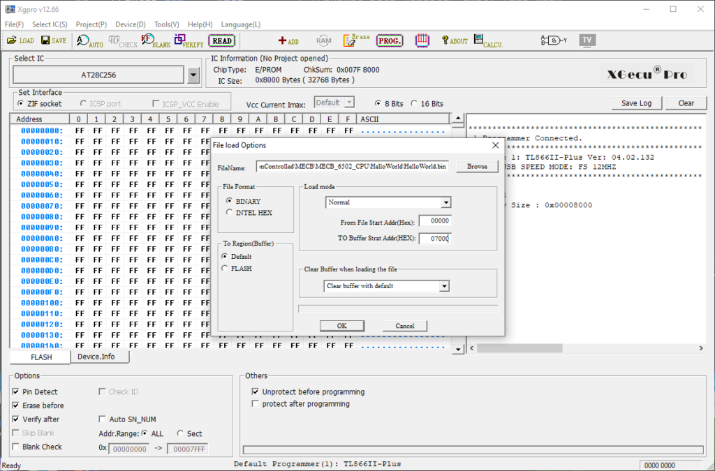
With the ROM programmed, I insert it into our 6502 CPU Card.
Our CPU Card is now fully populated, ready for it’s first test ever!
So, next I get it plugged into the backplane, and fire up our TeraTerm so we can monitor the serial output.
The, we were ready for the first turn-on!
So, how confident am I?
Well, with any new microprocessor project, you kind of have an expectation of some debugging required.
Note also, that with microprocessor projects, with their multiple bus connections, I’ve also modernised my prototyping approach.
Similar to how I’ve modernised my early 80’s Wire-wrap design, to now instead use my MECB PCB standard, I’ve also taken advantage of modern PCB design tools, and low cost PCB manufacturing, to modernise my prototyping process.
I now find that, particularly for microprocessor projects, instead of the usual breadboard prototype process, I find it more efficient to just dive straight into PCB routing and going straight to a PCB prototype.
So, instead of using a rat’s nest of jumper wires on a breadboard, and being impacted by breadboard capacitance & inductance, instead, I only have the possibility of a few cut PCB tracks, a few jumper wires, and perhaps a few PCB iterations.
But, this approach also fast-tracks the final PCB version, by getting into the PCB routing earlier in the design cycle.
Of course, the one down-side is you end up at moments like these. Where you’ve done all your design work, ordered and assembled the first PCB, and now, for the first time, you are ready to apply power and see what happens!
So, here goes….
Power on…
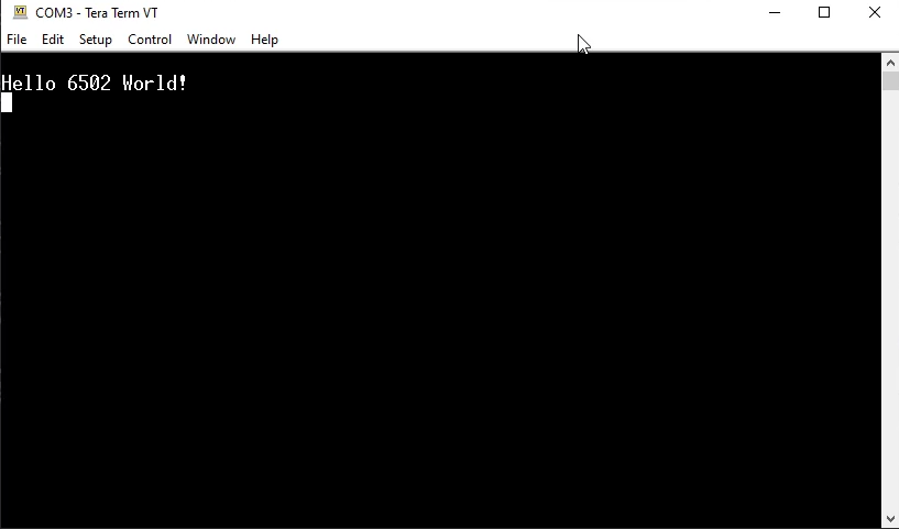
And, we have a successful Hello 6502 World!
Well, that’s pretty cool!
Okay, with that success, I next swap-out for an original MOS 6502 processor.
I take out the WDC chip, and also move the jumper across to the 6502 header.
Then, I insert one of my old MOS 6502 chips (sourced from AliExpress).
Plugged back into the backplane, and powered-on again.
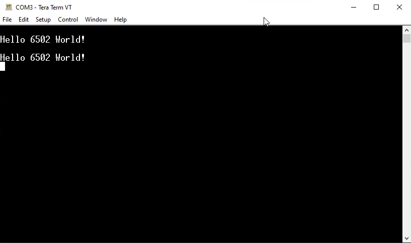
Awesome, we are still in business. As I expected, there was no need to update the PLD for the clock source when using an original MIS 6502!
Well, with that awesome success for our initial MECB 6502 CPU Card test, I think I’ll end this post / video here.
If anyone is interested in playing with their own 6502 on the MECB Bus, with the MECB 6502 CPU Card now tested working, you’ll now find it available from my Tindie Store.
You’ll also find resources on the MECB Github repository.