
Having recently completed a 6502 CPU Card for the Minimalist Europe Card system, I now have all of the system Cards that I need, for re-creating the early 80’s CreatiVision Console.
Join me as I describe the CreatiVision’s memory map, then configure & test CreatiVison code running (unchanged!), on the MECB based re-creation.
Those of you who have been following along with the evolution of my MECB based flexible system design, will know that I earlier mentioned that I was keen to re-create a CreatiVision console.
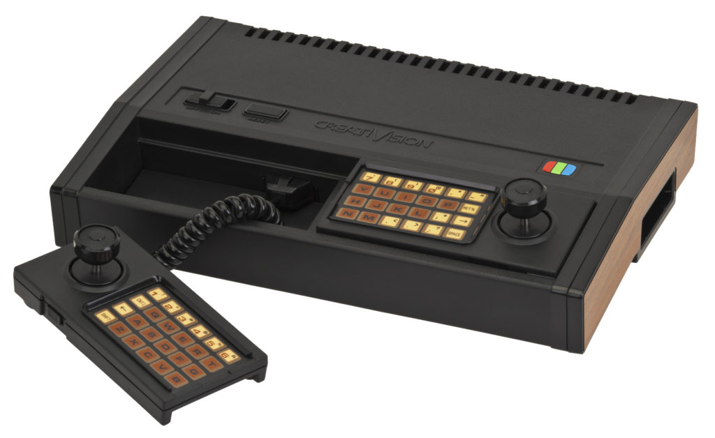
The CreatiVision was a colour TV console based on the 6502, the TMS9929 Video Display Processor, and the SN76489 sound generator chip.
Note that I’m calling this a re-creation, not an emulation!
This is because the intention is to re-create basically the equivalent hardware, that was used in an original CreatiVision. Nothing is being emulated here!
In theory, by configuring the original Retro hardware on our MECB system, to mimic the address-map of an original CreatiVision, we should be able to just run CreatiVision software, unchanged!
So, first-off, let’s take a closer look at the CreatiVision’s design and address map.
Here is the initial schematic of a CreatiVision, which includes the CPU, address decode and TMS VDP interfacing.
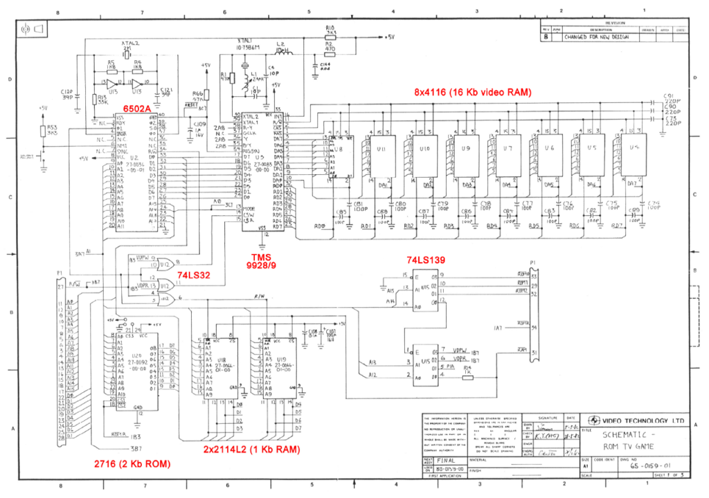
As was typical in the design for this type of mass market consumer device, a number of shortcuts were taken in order to save on costs, by minimising the number of parts needed.
With the CreatiVision, a couple of things are worth noting.
Firstly, the address decoding is achieved with just a single 74LS139 dual 2-line to 4-line decoder chip.
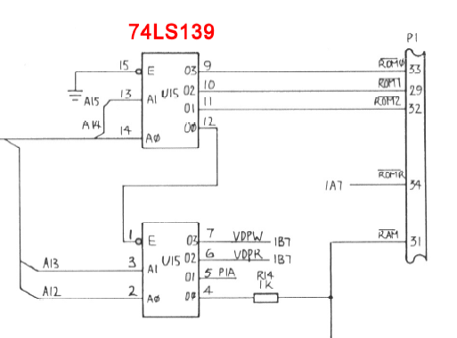
The first decoder in the chip splits the 6502’s 64K memory space into four 16K segments.
The lowest 16K segment, is then further split into four 4K segments, by the other decoder in the chip.
The top three 16K segments are labeled ROM2, ROM1, and ROM0, which was clearly intended for up to 48K or ROM in the address map.
The four 4K segments at the bottom of the address map, are firstly for the Static RAM, then we have labeled PIA, VDPR, and VDPW.
So, we have a 4K segment for RAM. Noting that the CreatiVision actually only has 1KB of SRAM onboard, via two 2114 1Kx4 Static RAM chips.
As the 1KB of SRAM is address decoded as a single 4K address space, the contents of the 1K RAM is effectively replicated 4 times.
A Motorola MC6821 PIA is used for the I/O. The PIA only requires 4 addresses, but it is also allocated a full 4K of address space. Rather wasteful!
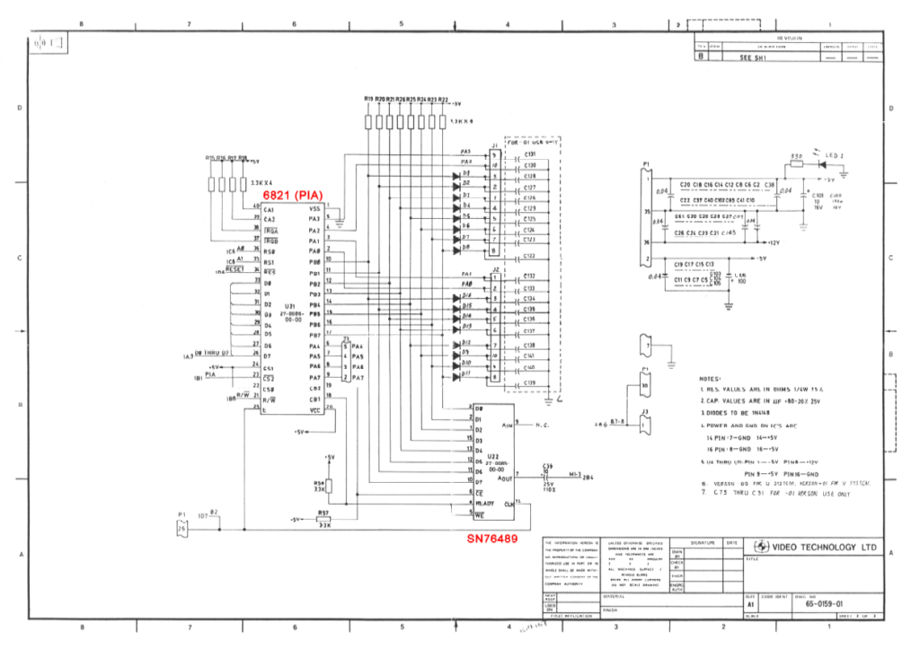
Similarly, The TMS VDP is allocated across two 4K address spaces. So, it is essentially using up a full 8K of the 64K available address space, even though a TMS VDP chip only actually requires 2 address locations.
Massively wasteful! But a very simple one chip address decoding solution.
This is the result of cost saving design, effectively minimising the decoding logic to save on chip count, but resulting in a large wastage of the address space.
But, probably the most concerning thing, in terms of the effect of cost saving design, is the VDP Read and VDP Write decoding logic.
In addition to the decoding of the two 4K address spaces, only two 74LS32 OR gates are used to then just gate these Chip Select signals with the Phase 1 clock output of the 6502, to create the VDP Read and Write chip selects.
Now, this simplicity means that the CPU’s Read/Write signal is not included in the TMS chips Read or Write selection logic.
This means that if the software were to inadvertently Write to the VDP Read 4K address space, it would actually be creating a hardware bus driver conflict, between the VDP’s data bus output drivers and the CPU’s data bus output drivers.
Not a good situation, when software can create potentially damaging output driver shorts!
So, with that brief analysis of the original CreatiVision address decoding logic, let’s take a look at what the memory map looks like.
I’ve put together this simple spreadsheet to summarise how the 64K address space of the 6502 CPU is split up. We can use this to configure our MECB Card address decode PLD logic.
Also, one other thing to take note of (from the CreatiVision schematic), is that the MOS 6502 CPU is clocked at 2Mhz.
So, to re-create a CreatiVision on MECB, I just need the 6502 CPU Card, the TMS VDP Display Card, and a Motorola I/O Card with Sound!
This gives us all the hardware that we need to run CreatiVision code.
For the 6502 CPU Card, I’ve first inserted a 2MHz Oscillator. In theory, we could also use a faster clock speed as the game speed is generally controlled by the VDP frame sync interrupts (50 or 60 interupts per second).
Then, let’s take a look at the WinCUPL address decode logic.
We’ll start with the 6502 CPU Card’s PLD chip select logic.
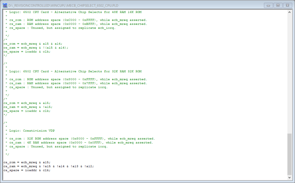
As you can see I’ve defined a chip select logic block for the CreatiVision.
In this case, I’ve assigned 4K of RAM to the bottom 4K of the address map $0000 to $0FFF.
For the ROM, I’ve initially just allocated the top 32K of the address map $8000 to $FFFF.
This is because I’m using a 32KB AT28C256 on the CPU Card, so we may as well just use it all!
Note that my intention (eventually), is to utilise the MECB 1MB ROM Expansion Card.
In that case (for the ROM Expansion Card), I would disable the CPU Card’s own onboard ROM, and instead allocate the full 48KB memory map ROM space allocation, to the 1MB ROM Expansion Card.
This would then allow up to 16 switchable 48KB banks on the ROM Expansion Card, to allow us to switch between 16 different CreatiVision cartridges. Nice!
For now, the 32KB of onboard CPU Card ROM, will enable us to test our re-creation is actually working, before adding in the expansion card.
Next, lets look at the Motorola I/O Card PLD address select logic.
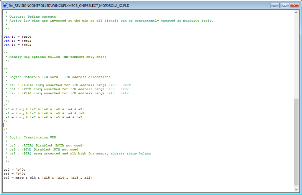
For the I/O Card we only need the PIA. Note also, that the PIA is memory mapped for the 4K address range $1000 – $1FFF
Finally, we have the TMS Video Card PLD Select logic.
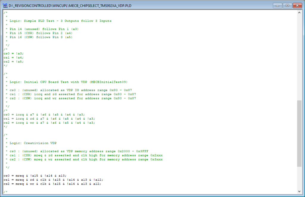
For this, I’ve memory mapped the VDPR (CSR) and VDPW (CSW) addresses, as per the memory map.
However, I’ve also added the Read & Write signals (rd and wr), to protect against the CreatiVision’s potentially damaging driver conflict, from inadvertently writing to the VDP Read address range.
Okay, with three newly programmed PLD’s, I then get them inserted in the MECB Cards.
Next, we need to program our ROM.
First we have the CreatiVision’s BIOS, which is a 2KB 2716 ROM image, that we’ll need to load at the top of our 32KB ROM space.
So, in our programmer, we’ll load the 2KB bin file into the 32KB buffer at $7800.
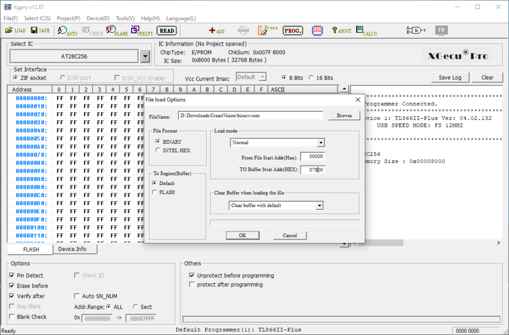
Next, I’ll load the CreatiVision’s Space Invaders game “Sonic Invaders” ROM image. It is a 4KB game cartridge.
Now, I understand that the 4KB Game Cartridges are expected to be located at $B000 – $BFFF.
So, we’ll add the ROM Image to the programmer buffer at offset $3000.
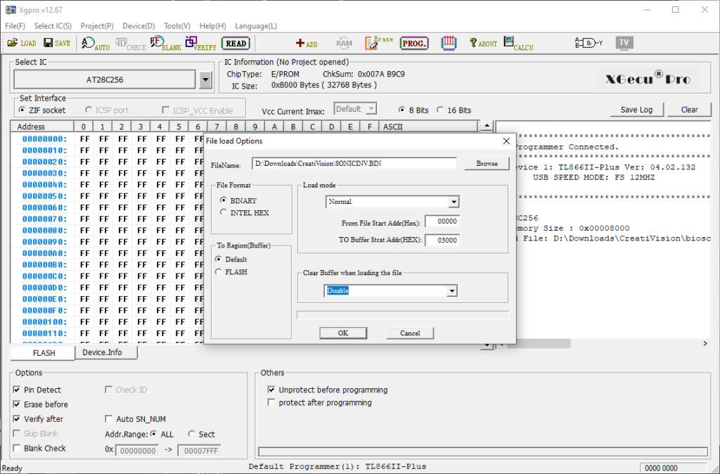
Now, with the ROM programmed, I then get that inserted in our MECB 6502 CPU Card.
Finally, I plug in my sound system, for the expected Retro game sound effects!
Finally, we should now be ready to apply power and see what happens.
Here goes…
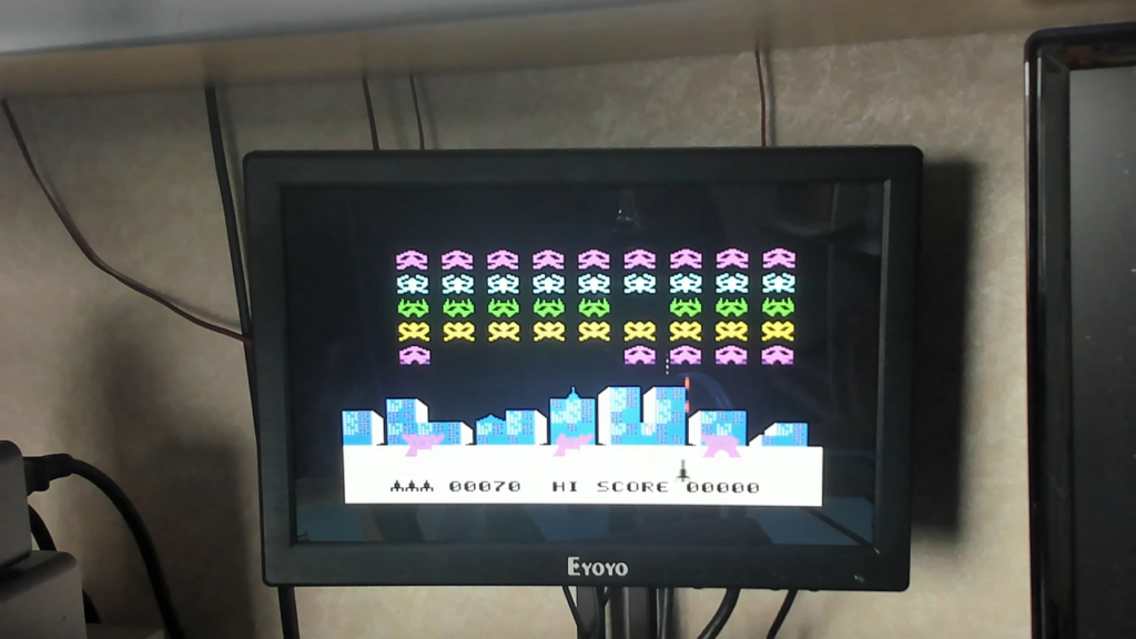
And, we have success! Sonic Invader is running! And, it looks and sounds awesome!
Be sure to watch the video to see & hear it in action!
In summary, we have a verified CreatiVision re-creation!
Now, note that “Sonic Invader” is running in Attract Mode, as I don’t yet have any controller input.
So, with this success, the next step will be to interface some controllers, so that I can actually play some games.
But, I think that’ll do for Part 1. So far so good!