
Recently I published a post / video, covering some PLCC packaged CPU chips that I’d received as a donation from Lez Anderson.
In that video, I built a custom PLCC to DIP40 adapter, to allow me to test the CPU chips in my existing 6809 CPU Card. I’ve also made this adapter available on my Tindie Store, just in case that’s of assistance to anybody else.
I also mentioned that I would add a project to my to-do list, to make a PLCC version of my existing 6809 CPU Card. At the same time, taking advantage of the PLCC space saving to combine it with the ROM Expansion Card.
This post / video is therefore a follow-up, to present my now completed PLCC based CPU Card project.
This project actually took me a bit longer than I originally thought it would.
Primarily, because I dived into the project with grand thoughts of making a single, combined, DIL package or PLCC package CPU Card, also allowing building with or without ROM expansion (phew!).
Effectively, making it a v3.0 update to the existing 6809 CPU Card, to add the PLCC packaged CPU footprint to the existing Dual In-Line Package footprint. Also, with PLCC based ROM expansion added to the existing Dual In-Line Package ROM footprint.
So, basically, an all-options-in-one 6809 or 6309 CPU Card.
Because this made for a pretty busy PCB layout, for my standard MECB PCB size, it also forced me to go to a 4 layer PCB design.
Now, this was a fun KiCAD project to put together and layout.
But, this is actually a good example of what can happen when you’re working on your own, and don’t have a collegue to bounce your ideas off.
Specifically, you can head-off down the path of what you think was a great idea, without first stepping back to sense-check that what you are doing actually does make sense!
So, after 2 days of PCB routing, when I was about 90% finished with my 4-layer all-in-one combination PCB creation, I finally took a moment to check the ordering process for the first prototype PCB manufacture.
It was only then, that I realised that the “little bit more expensive” 4-layer PCB, was actually going to cost me 4x (four times!) the price of my usual 2-layer PCB’s. And, even if I went to a higher production quantity, I was looking at 3x the PCB cost!
Only then did it dawn on me that anybody obtaining the PCB (for their own build), would either be building a DIL packaged CPU based system, or a PLCC CPU based system. Obviously not both!
So, from an end-user perspective there is no real advantage to a “all-in-one combination PCB” (that would justify the increased PCB cost!).
I think my desire to make it this way, was purely from a simplified stocking (or inventory) point of view. And, of course, “The Challenge!“
I’d then have just one PCB, to suit both DIL package and PLCC packaged build desires.
So, roll-on the next day, and I started-over again, on a 2-layer PLCC only CPU Card. Still enabling the combination of CPU Card and ROM Expansion Card, but no longer supporting a choice of either DIL or PLCC packages (for the CPU & ROM).
This, of course, does mean a separate 6309 PLCC based CPU Card being added to the available MECB Cards. With the existing 6809 CPU Card remaining available.
But, as I said, this does actually make more sense (from a user perspective), and the additional PLCC CPU Card PCB will cost the same as the usual 2-layer PCB price.
In case you’re curious about this journey I went on, here is a 3D PCB render of what my 90% complete 4-layer all-in-one combination PCB looks like!
I think it’s pretty nice (even a work of art). But, it will remain as a 90% complete project (on hold, for now), as I simply can’t justify completing it and ordering any PCBs!
So, here is the 3D PCB render of the eventual, and more appropriate, 2-layer new 6309 PLCC based CPU Card.
Okay, let’s now take a look at the schematic.
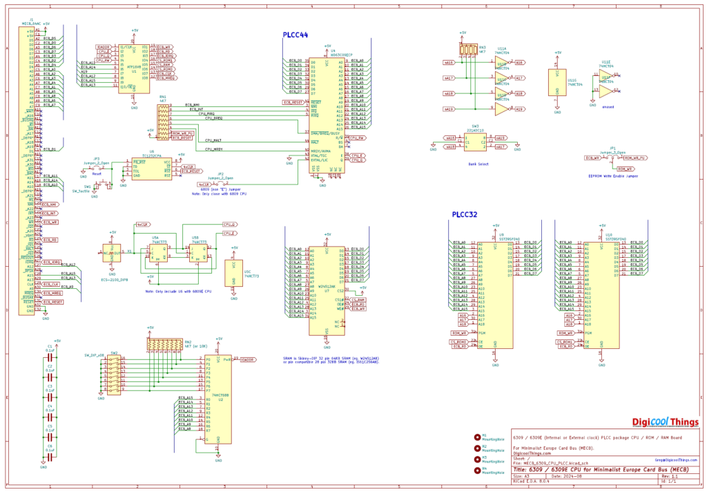
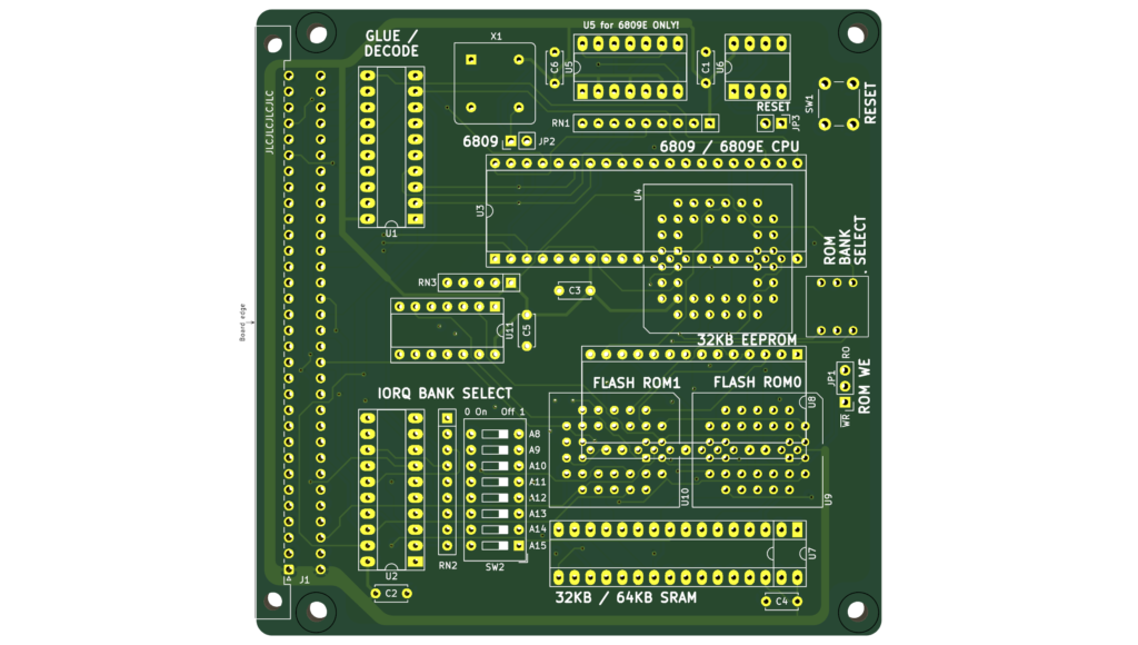
This is basically a mash-up of the 6809 CPU Card and the 1MB ROM Expansion Card. Just, with the CPU and ROM packages changed to PLCC footprint, and an update to the Bank Select switch that I’m using.
The switch used on the existing ROM Expansion Card is quite expensive, and only readily available from a limited number of suppliers.
it’s a nice rotary coded switch, but I thought I could do better. So I spent some time researching the options, and buying a few samples to check the quality.
First off, I transitioned to a 6 pin 3:3 layout switch footprint, instead of the existing 5 pin 4:1 layout.
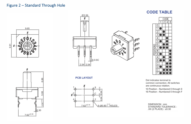
This provide a more mechanically robust solution, as the 4:1 pin layout does put extra mechanical stress on the single pin side of the switch mounting.
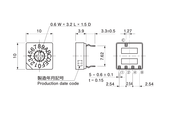
In addition, I found that positive logic switches are more readily available, than the negative logic variety that I had been using.
A small downside of this change to positive logic, is the need for an inverter when using the rotary coded switch in the common configuration of switching-low, address lines that are otherwise pulled-high. Effectively, with a switch On, it connects the pulled high signal to Ground. Hence the reason why negative logic switches are convenient.
However, this buffering with an inverter also has the advantage that with the switch omitted from the circuit, the resulting address lines are all driven low (or, bank zero). So, if ROM bank switching wasn’t required, you could just leave out the rotary coded switch, using only the first bank of the ROM.
Note that, as with the ROM Expansion Card, you can also choose to use 1 or 2 ROMs, depending on whether you need 8 or 16 switched banks of up-to 64K each.
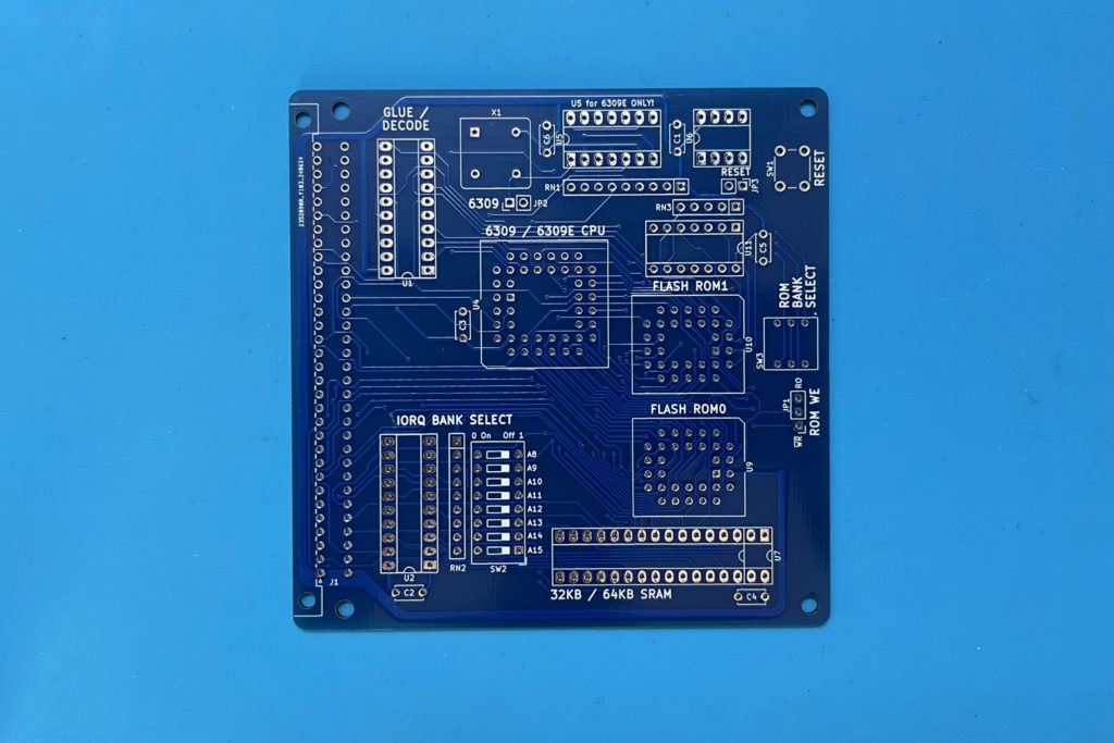
So, here’s the first manufactured v1.0 PCB.
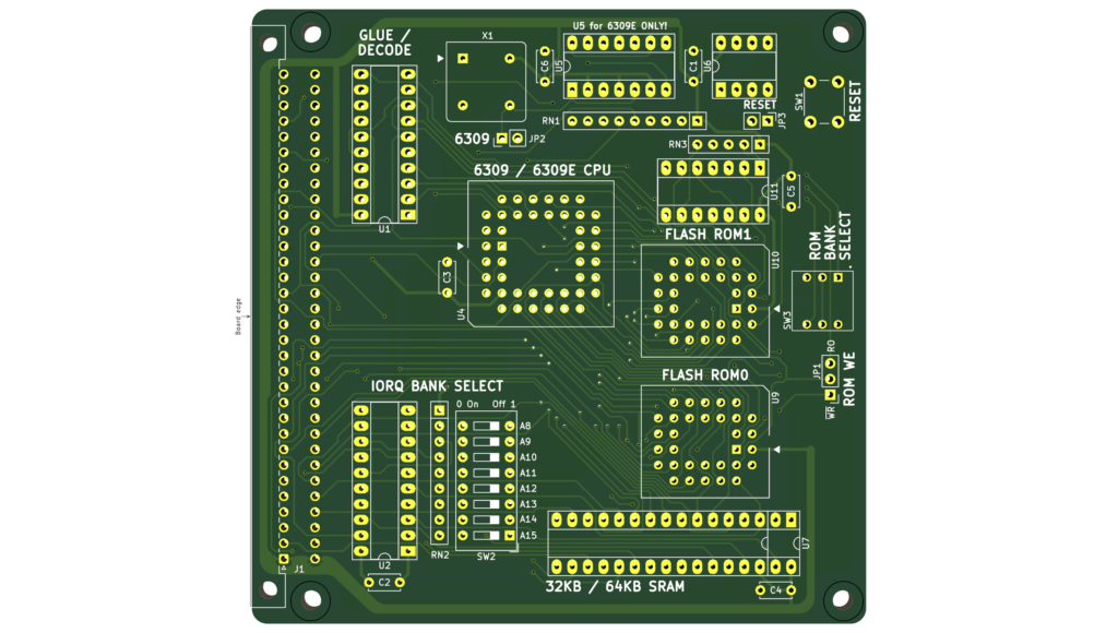
Time to put it together… And, we now have our first assembled card.
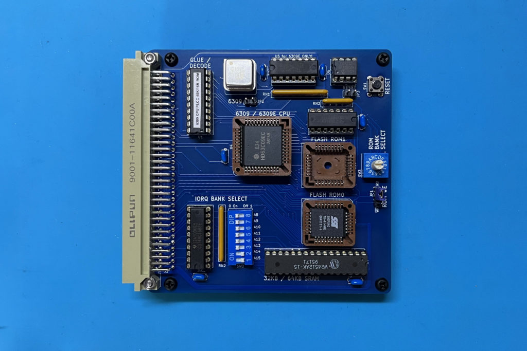
I think it looks really nice, with it’s PLCC socketed chips, and a configurable 64K memory map with your choice of the RAM and ROM address space mix.
Okay, now that we have an assembled Card, it’s time to test it.
Now, this is using a 3MHz rated ‘C’ version of the 6309 CPU (the HD63C09EC). However, based on past experience, I actually drop in a 16Mhz oscillator, so we’re running overclocked at 4Mhz CPU speed.
With the oscillator in place, let’s take a look at the PLD code.
Here’s the first page of the WinCUPL source for our 6309 PLCC CPU Card:
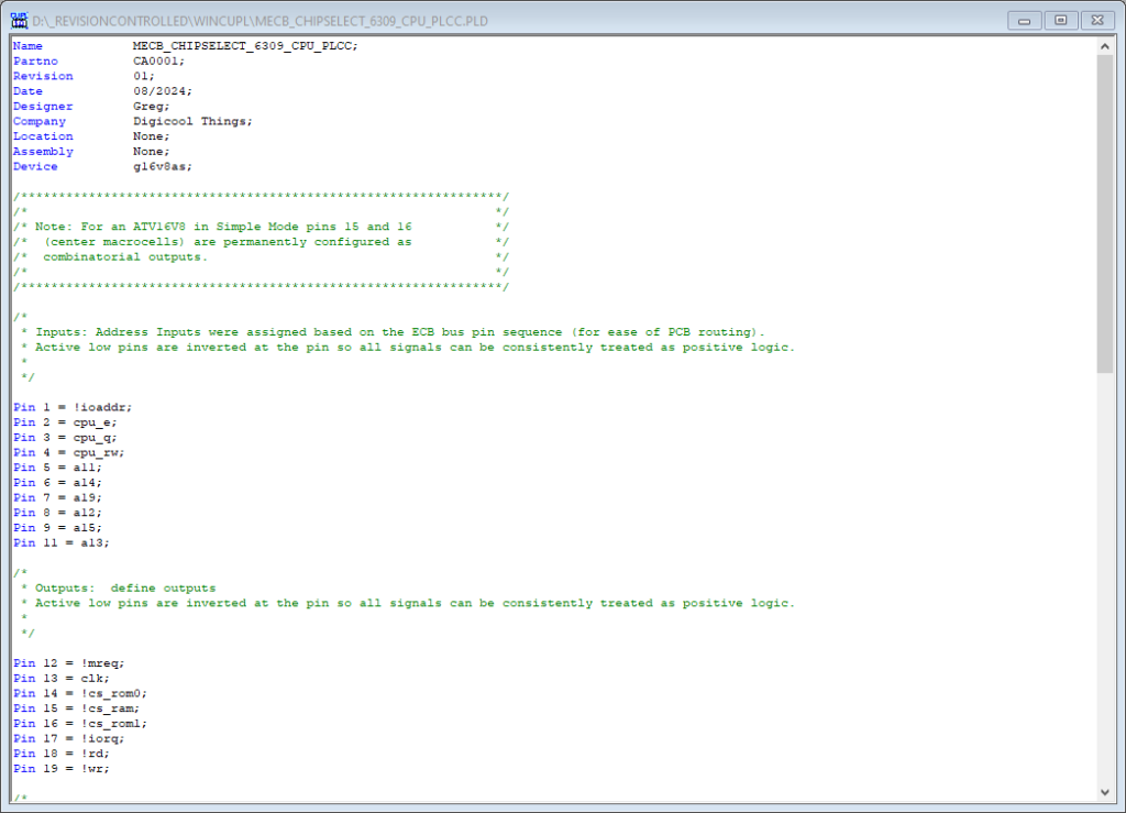
Again, this is really just a mash-up of the existing 6809 CPU Card and 1MB ROM Expansion CPU Card.
The only real difference from the 6809 CPU Card, is that I’ve substituted the lowest A10 address line input, for our switched A19 address line, to allow switching between our two 512MB ROMs. Also, the previously unused 3rd Chip Select output (pin 16), now becomes the second ROM Chip Select cs_rom1
I’ve created some commented-out Chip Select logic for 56K RAM 8K ROM, and also 32K ROM & RAM memory maps. But, for now, I’ve enabled the 48K RAM 16K ROM address map.
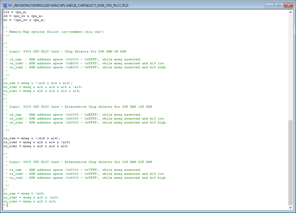
This just leaves the ROM. For the ROM, for the initial test, I’ve just used the same ROM image that I have used for the existing 1MB ROM Expansion Card. This has the ASSIST09 monitor in bank 0, and 6809 Extended BASIC in bank 1, leaving six banks free (in ROM0), for whatever we might want to later add for easily accessible use.
With both the PLD glu logic explained and a PLCC Flash ROM programmed, we’re almost ready for our first test.
First I make sure that we have the I/O bank select switch set for $CO, as expected by our existing ROM code. I also install a jumper for ROM Read Only.
Now, we’re ready for our first power-up!
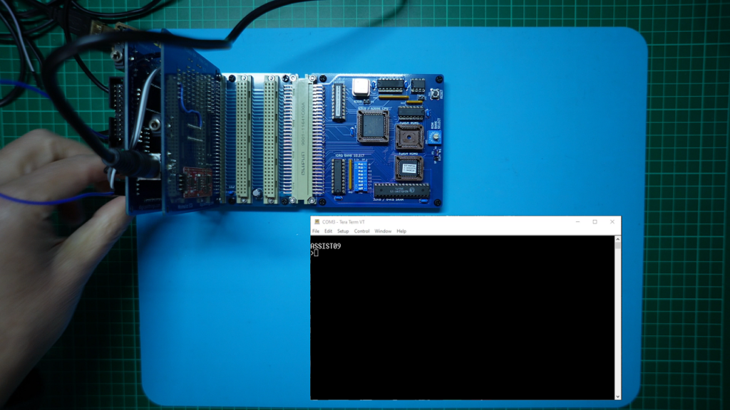
And, we have a successful ASSIST09 prompt.
To be sure, I switch-off and change from ROM Bank 0 to Bank 1.
Then, apply power again…
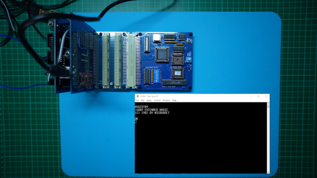
And, we have a successful 6809 Enhanced BASIC prompt.
So, I’m pretty happy with my first Retro friendly, Through-Hole only, PLCC CPU Card.
In fact, I’d say it’s my new favourite CPU Card!
If you’d like to build you own, you should now find it on my Tindie Store, with the usual options of the PCB only, or, there are various optional packs for the parts you may not already have in your parts drawer.