
After a break over the new year holiday period, I’m back with my first blog / video for 2026.
This blog / video covers something exciting, that I’ve been working on over the holiday period, and something that I also mentioned in my last video.
It is, of course, the new Motorola 68008 CPU Card.
Join me, as I walk through the design, assembly, and using this new powerful CPU Card.
Introduction
This Card features the relatively powerful 16/32-bit internal Motorola 68008 processor, together with up to 2MB of linear addressed on-board memory, as well as compatibility with the MECB bus.
This allows using existing MECB peripheral cards, and also allows further expansion of the memory via MECB (if required).
The 68008 CPU Card builds on some excellent work originally done by Forum member Emil, who created an initial v1 card.
With Emil’s permission I’ve now taken his design to v2, with the expansion of the card to now carry up to 2MB of memory, and also to be based on a single larger CPLD device, to deliver the slightly more complex glue logic required by the 68008.
This CPU Card is likely to be the most powerful CPU Card designed for the 8-bit MECB platform. Effectively shoe-horning a 16/32-bit processor onto an 8-bit bus.
But, more importantly, this CPU card provides the means to experiment with the 68K ISA (Instruction Set Architecture), on our MECB platform.
Schematic
So, let’s first dive into the schematic.
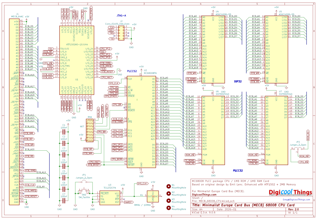
As you can see, it’s relatively simple. Along with the CPU chip, in its PLCC52 package, we have two 512KB RAM chips, and two 512KB FLASH ROMs.
In addition we have a single PLCC44 packaged CPLD chip.
Pretty much just leaving the clock and reset circuitry.
One key feature was using the PLCC52 packaged 68008 CPU, instead of it’s alternative DIP48 package.
The benefit of choosing the PLCC package, is that the extra pins are used to enable a 4MB linear addressing space (with 22 Address lines), instead of the 1MB / 20 address line limit of the DIP48 packaged version.
This has enabled allocating a whole megabyte to RAM memory, a further megabyte to ROM memory, while also leaving a full 1MB of space dedicated to the MECB memory request (MEMRQ), and even allowing the MECB I/O request (IOREQ) it’s own space, without stealing from the memory address space allocation.
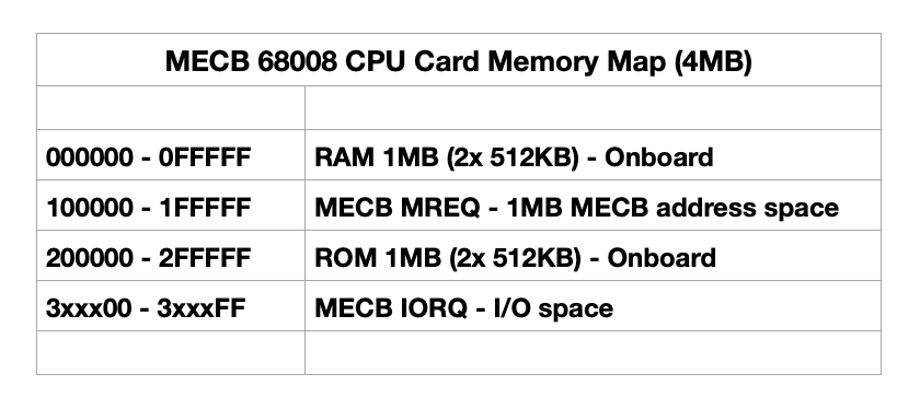
Also, as we have plenty of memory space to play with, it is probably unnecessary to need to modify the CPLD for the purpose of re-defining different memory maps, as we do with the other 64KB address space limited 8-bit CPU Cards.
Even so, the CPU card includes a JTAG connector, to allow in-circuit re-programming of the CPLD.
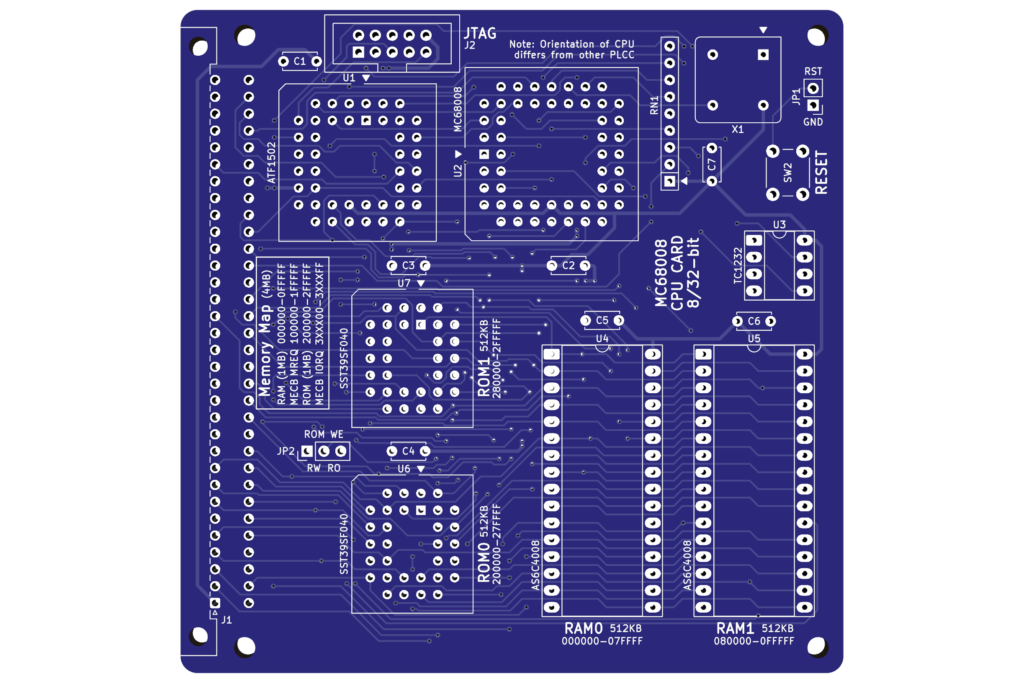
PCB Layout
So, let’s now take a look at the final v2.0 PCB layout.
Here is a 3D render of the PCB.
This is actually the 3rd iteration of this PCB, until I was finally happy to call it ready for release.
The first version of the PCB, was shown on my previous video. It included an additional logic chip, which was an intended temporary addition, to assist with my development and debugging of the final CPLD logic code.
This additional chip has now been removed, and the final iteration just building on the second iteration’s device positioning and trace routing optimisations.
As you can see from the PCB render, I’ve also spent time on the silk-screen, to also document the memory map, and make assembly as easy as guided as possible.
Overall, a lot of hours have gone into the final PCB creation, and I’m really happy with how its turned out.
So, on my workbench you can see all of the parts laid-out ready for assembly.
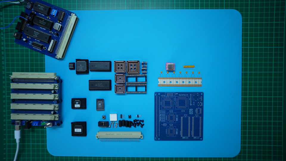
As I’ve done with all of my recent projects, I’ll be offering all of the parts on my Tindie store, so you have the ease of ordering a complete kitset, meaning you just need to assemble it (and not have to worry about sourcing parts).
The out-of-production parts (in this case the 68008 CPU itself), have been sourced and tested as working in my own Card, before I ship them to you.
I’ve found an approximate 10% – 20% failure rate on sourcing these out-of-production recovered parts. So, hopefully this pre-testing will assist anyone keen to build their own 68008 CPU Card.
Of course, the full kitset is offered via multiple “optional” component packs.
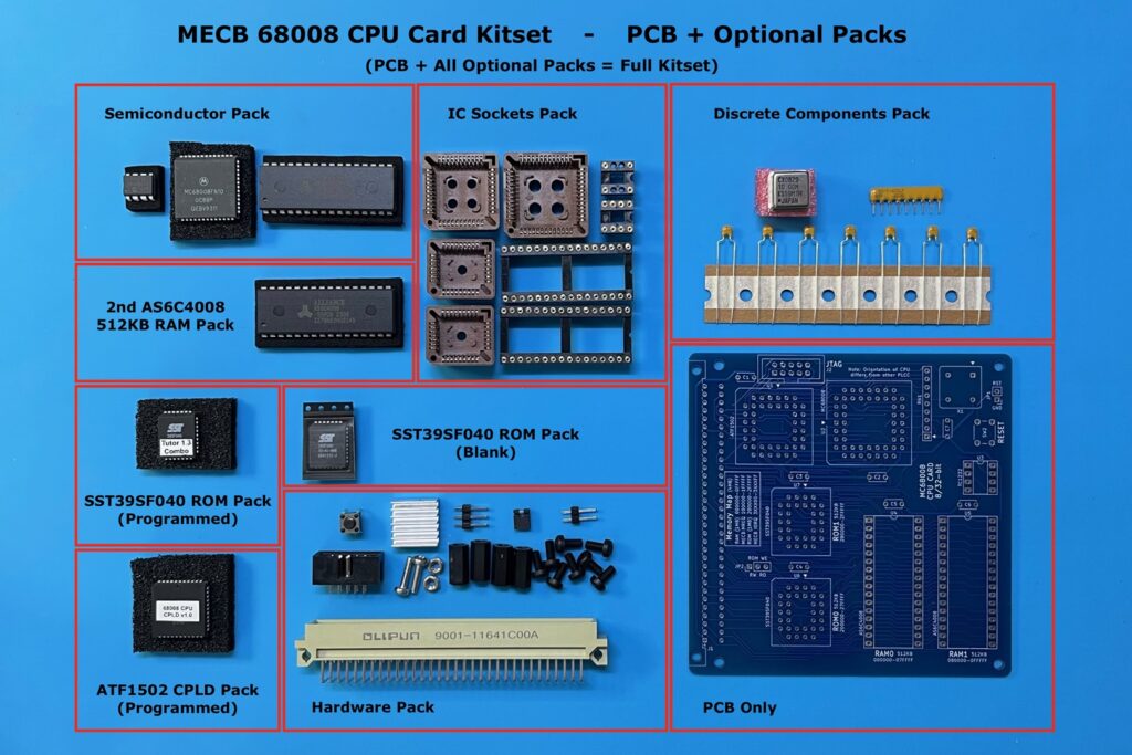
So, you have the choice of just ordering the PCB, or ordering whichever packs are helpful to you, or, ordering all packs for a complete kitset.
PCB Assembly
So, lets get the first one assembled (please watch the earlier linked video, for the assembly sequence I used).
With all the soldering now complete, I next get all the IC’s inserted, including the pre-programmed CPLD, and ROM.
Please watch the video for the initial power-on test.
Now that we’re up and running, I thought I’d start out by doing a thermal check, before we progress any further.
After all, this is a higher power 16/32-bit internal processor, running at 10MHz.
So here is the result of taking a thermal image of the card while operating.
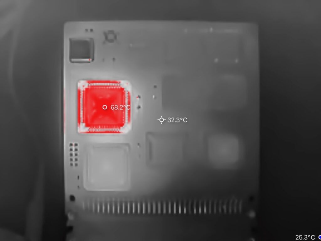
Firstly, it’s good to confirm that there are no thermal issues elsewhere on the PCB design.
But, the 68008 CPU package itself is measuring 68.2 degrees celsius, which is running pretty close to the maximum of the specified operating temperature range, of 0 degrees to 70 degrees celsius.
To help mitigate this, I’ll use a radiator heatsink, which provides a solution for drawing heat away from the chip, to a much bigger surface area, for helping to radiate that heat.
First, I’ll clean the top surface of the PLCC chip with some Isopropyl alcohol, then I can peel-off the thermal tape cover, to stick the radiator heatsink to the top of the chip.
Now, after giving the chip time to reach it’s operating temperature, let’s take another thermal image.
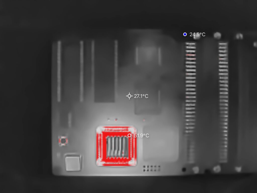
Okay, now things are looking a bit more comfortable. The IC body itself is now showing below 60 degrees, and the heatsink is feeling hot to touch (inidcating it is doing it’s job of transfering the heat away from the IC body).
CPLD Glue Logic
Now, I thought that next-up, I’ll show you the CPLD source code.
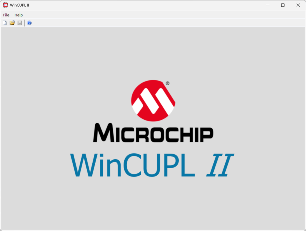
I’ve created this using the recently released, and free, WinCUPL II software, from Microchip.
The .pld source, and also the pre-compiled .jed file, ready for programming into an ATF1502 CPLD, are available on the DigicoolThings MECB Github repository.
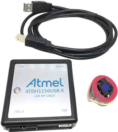
Now, unlike the smaller ATF16V8 and ATF22V10 PLD chips, the larger ATF1502 cannot simply be programmed directly in a common TL866 USB programmer.
Instead you need the appropriate Microchip programming utility, and a compatible JTAG in-circuit programmer cable.
I use the official Microchip ATDH1150USB JTAG cable. But, I understand that 3rd party cables work just as well.
Alternatively, I do offer the CPLD chip pre-programmed, via my Tindie store.
Okay below is the beginning of the source code. Please either refer to the following, while reviewing the .PLD source code file, or, watch the video for a visual walk-through.
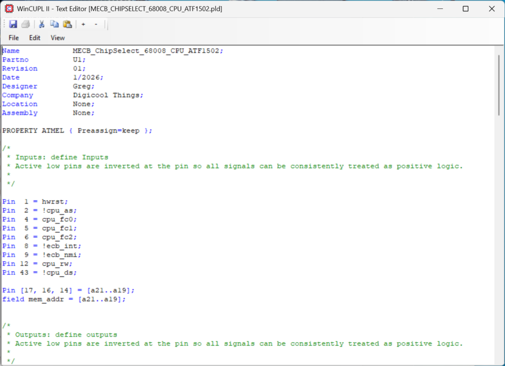
You can see that I allocated the pins, to the relevant signal named variables, keeping everything in consistent positive logic.
I also created a field as mem_addr, to simplify the later chip select address range logic.
Next, I implement the Interrupt Control, which is simply translating the MECB NMI and INT signals to be level 7 and level 1 of the 68008’s three pin Interrupt Priority Level inputs.
Next we simply split the CPU’s combined R/W signal into the bus’s separate Read and Write signals.
Then we have the on-board RAM and ROM chip selects.
The key point to note is the ‘vector’ variable. This is defined later on, and is used for moving ROM0 into the RAM0 address space during the initial reset sequence.
Next we have the bus Memory Request and I/O Request memory address ranges defined.
Noting here that the Bus I/O Request also defines the CPU’s VPA (or Valid Peripheral Address) input, which tells the 68008 to perform a 6800 peripheral compatible addressing cycle.
Then, I define the CPU’s data acknowledge (DTACK) input signal, whenever there is a data strobe for a valid memory access.
Next we have the hard reset control.
Of note here is that for the 68008 a hard reset is initiated by pulling both the Halt and Reset bidirectional pins low.
As these pins are bidirectional, these CPLD pins must effectively be open-drain outputs. i.e. Tri-state when not asserted.
Therefore we also use the Output Enable extensions, to only enable the outputs when hardware reset is asserted.
Lastly, we have the magic that defines the ‘vector’ variable (mentioned earlier).
The logic is implemented to create a 4-bit counter, such that we can count the first 8 rising edges of the CPU Address Strobe, following a hardware reset.
These first 8 Address Strobes are the CPU accessing the initial Supervisor Stack pointer and the initial Program Counter 32-bit register vector values.
These are fetched from the first 8 bytes of memory. Therefore the purpose of the “vector” variable is to indicate when we should temporarily substitute the ROM0 and RAM0 memory spaces, so that the vectors are retrieved from the beginning of ROM.
Right, there you have it. A little more complex than our usual 8-bit CPU glue logic, but a perfect fit for the larger ATF1502 CPLD.
TUTOR 1.3 Monitor / Debug
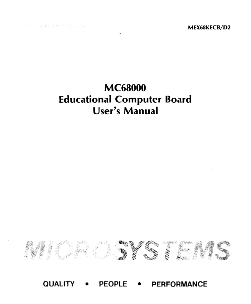
Next, I’ll point you to the Tutor monitor guide, which you’ll find in the Motorola MC68000 Educational Computer Board user’s manual.
The PDF of which I have uploaded to the MECB Github.
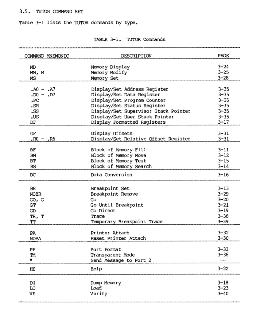
As an example here is a quick summary of the mostly 2 character Tutor command set.
To experiment with the new CPU card we can write our Assembly Code programs using a cross-assembler, and then transfer them to the 68008 CPU card via the TUTOR Load command, then run them with the TUTOR Go command.
Once debugged, we might then choose to Assemble and Program them to ROM.
VASM Assembler
For developing programs I use the free Microsoft Visual Studio Code, with the VASM Motorola 68K cross assembler.
Here is an example of the Terminal Scripts I have setup in my Visual Studio Code, to simplify the development cycle.
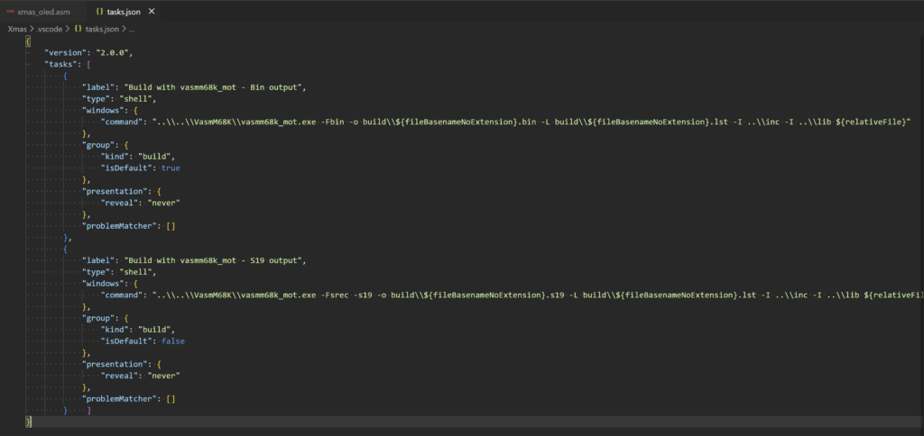
In this way I can just run a Visual Studio Code build of my code, and I have a .S19 file ready to transfer across to the CPU card for testing.
Christmas Demo (xmas_oled.asm)
To demonstrate this, I have borrowed Emil’s conversion of my original 6809 Christmas Demo of the Motorola I/O Card’s sound generator and TMS9918 series Video Display Generator display card.
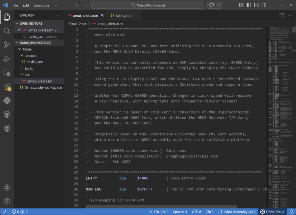
Emil converted the original 6809 code to run on the 68008, and to also utilise the MECB OLED Display Card, instead of the TMS VDG Display Card, that I originally used.
I have just made some modifications to the note frequency table, for our 10MHz CPU clock, and also made a simple stand-alone source file for our test / demonstration needs.
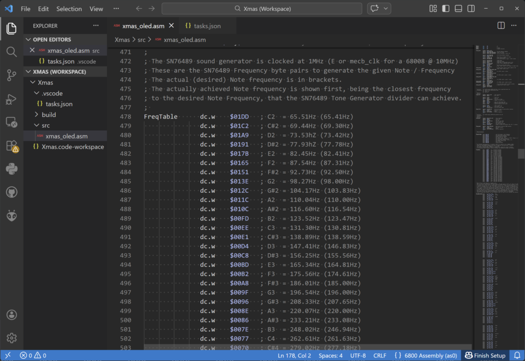
You’ll also find this version on the DigicoolThings MECB Github.
Before proceeding, I’ll just mention that this Christmas Demo provides quite a good test, as the program drives the Sound generator chip, via the PIA port B, and is also using the 6840 Timer to generate a 20ms CPU Interrupt, which delivers the music notes etc. Also, we are driving the 8-bit OLED Display Card via another I/O port.
To try this out, I’ll first install an OLED Display Card onto our backplane, and set-up a camera to capture the display output on my video. I’ll also connect the audio out from my Motorola I/O Card to my sound system.
Finally, I’ll then build the .S19 file, and I’ll transfer it over to the 68008 card.
Trying some TUTOR Monitor Commands
With that done, let’s try some of the TUTOR commands (please view the video for the following demonstration).
Firstly, we can display all of the CPU registers with the DF command.
And we can see the Program Counter is currently set to 00000000.
We can also inspect the beginning of our program by using the display memory command, from location 4000, with the MD 4000 command.
We can compare this to our Assembly listing, and we can see that the first instruction, at 4000, loads the A7 register (Stack pointer), with the Address 0007FFF0. And, the second instruction is located at address 4006.
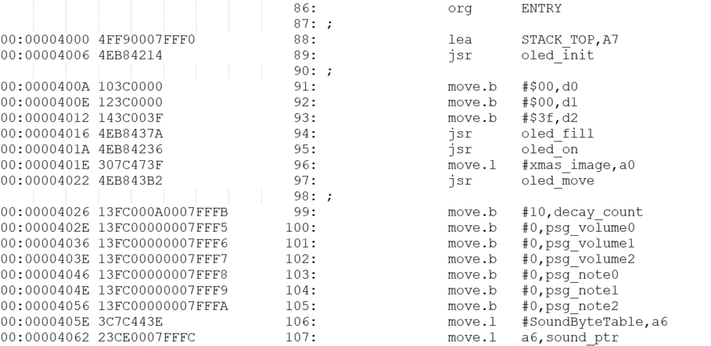
So, for demonstration purposes, I’ll create a Breakpoint at 4006, using the BR 4006 command.
I can also set the Program Counter to 4000 using the .PC 4000 command, and then check it with the DF command to display all the registers, as before. Now we can see the Program Counter is set to 4000.
So, having set this up, I can now run our program from the Program Counter address, by simply using the GO (or G command for short).
Running Our Christmas Demo
Okay, lets try that out (be sure to watch the Video for this demonstration!).
And, as expected, the program stopped at our 4006 breakpoint (as indicated by the Program Counter, and the BREAKPOINT indication).
Also, we can also see that register A7 has been successfully loaded with 0007FFF0.
So, to continue our program I just need to GO again…
And, our Christmas graphics are displaying on our MECB attached OLED Display Card, and our Christmas tune is playing via out MECB attached Motorola I/O Card.
Awesome!
So, you now have a flexible platform for your 68K Assembly Code learning and experimentation.
In addition, Emil pointed me to a good book on 68000 Assembly programming, which is a good place to start, if you’re new to the 68000.
You can find the book here.
So, have fun, and I look forward to hearing more about your experimentation and creations! Be sure to join us on the Forum.