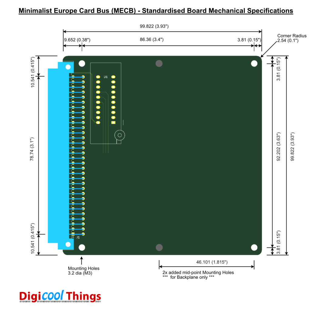
This follows on from my Backplane Design & Build for the Minimalist Europe Card Bus (MECB), where I walked-through the design of my MECB Backplane, and I then assembled my first Backplane, ready to connect together the MECB cards that I will subsequently design and build.
For this modular Bus based system, the first logical card to design is a Prototype card, which will assist prototyping further cards, and will also be useful for bringing out the bus connections for bus monitoring.
Join me, as I first walk-through the design of my first MECB Prototype card, and I then assemble my first card, ready to allow prototyping future cards and also can be used for point-to-point wiring for one-off builds of finalised card designs.
Background
It seemed logical to start with a Prototype card, as this can then form the basis for prototyping designs for other cards. In addition, it provides a simple way to expose the bus connector signals via a pin header for general testing or bus monitoring.
A prototype card can be used in the horizontal position, via the Backplane’s right angle connector, to assist with access during prototyping. Or, if it is ultimately used to create a permanent point-to-point wired custom design card, it could (of course) just be plugged into any Backplane slot as with any other pre-designed MECB card.
Design
As with the Backplane, the prototype card design started by creating a new KiCAD project based on the MECB Standardised Mechanical Specification KiCAD Template, that I had created earlier.

There was an initial thought that I’d keep the ATF16V8 Address Decoding / Glue logic PLD, that I’d included in the KiCAD template.
However, I decided to follow the KISS principle, and “keep it simple” for the first Prototype card design. I can always create a second Prototype card design later, if it’s decided that having the standard PLD included on the card would be beneficial.
Instead, my first Prototype card will maximise the space available for a perf-board grid of holes, for free use.
So, with that in mind, lets summarise the design parameters:
Prototype Design Parameters
- All dimensions and corner mounting holes, as per the MECB Standardised Board Mechanical Specification.
- A 64-pin header, clearly labelled with the A & C rows and pins 1 – 32, for ease of access to all bus signals.
- Power bus bars along the two sides of the card, to distribute the +5V and Ground power connections.
- All remaining board space (with exception of mounting hole clearance), to be utilised for free use through-hole pads, in a 0.1″ perf-board style grid.
Prototype Design Notes
- Header pins positioned directly alongside the DIN connector mounting holes, with 0.1″ spacing, to maximise available prototype grid area.
- Bus connector pin numbers only are labelled on the silk screen, as labelling with the actual signal names would consume available grid space.
Schematic
We start off by creating a new KiCAD project from the standard MECB template.
Then, we can delete the glue-logic PLD from the schematic, as we’re not including that in our first prototype card design.
Having deleted the PLD from the schematic, we then select “Update PCB from Schematic” (F8 hotkey), to also remove the PLD from the PCB layout.
On the PCB Editor we can change the selection filter to “Tracks” only, so we can then easily select and delete all of the existing PCB routing tracks, as they are no longer need.
At this point we then have the basis for creating a new MECB card, without a PLD device.
The Prototype card schematic can now be designed.
Firstly we fully label all 64 Bus connector pins, as we want to bring out all pins to the prototype board, even though for the Minimalist Europe Card Bus we are only using a subset of the ECB signals.
We then implement a 2 row by 32 pin header, which is simply linked one-to-one to the 64 pin DIN connector’s A & C rows.
Finally, we can use a couple of standard 2×2 connector symbols and associate them with some custom footprints that we create for the main grid, and for the two power bus bars running along each side of the board.

PCB Layout
For the PCB layout, the 2 row 32 pin header strip is position directly alongside the DIN connector, and the prototyping grid area is maximised. Also, we have the Ground & +5V power bars along the top and bottom edges of the board layout.
The header pin labelling fits efficiently between the grid holes, without consuming any grid space. The labeling is repeated on both sides of the PCB.


Assembly
You can view my linked Youtube video, which includes the full Assembly walk-through.
Next, well take a look at our first functional MECB card. But until then…
Links
MECB on GitHub – Board Mechanical Specification / KiCAD Template
