Michael wrote: Sat Jul 13, 2024 5:58 pm
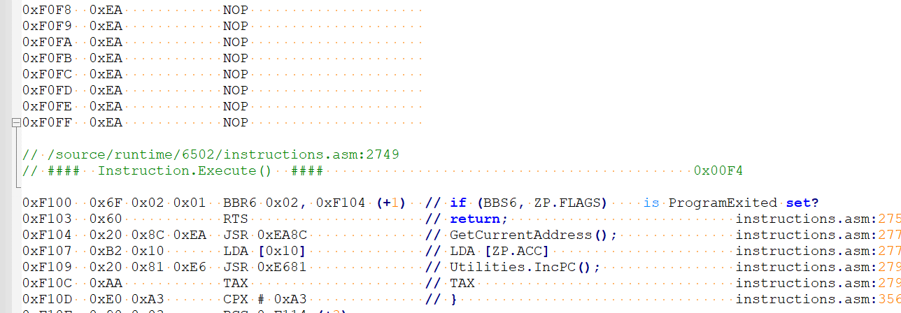
I've got my I/O mapped on the 6502 board to F0xx (A8..A11 on and A12..A15 off). This is working since I am both reading and writing characters via the ACIA (including Rx interrupt). Yay!
I assumed that mean that 256 bytes (F000 through F0FF) are mapped to I/O, correct?
My ROM straddles this range and I have code on either side. It appears that when I call my function at F100, things go sideways (hang).
That is correct.
In effect
the /IORQ bus control line takes priority over the /MREQ bus control line.
/IORQ itself is based on the /IOADDR named output of the IORQ Bank Select comparator (i.e. your DIP switch 256 byte I/O bank select settings).
This logic is all defined by the PLD logic statements, which provides the ultimate MECB Card implementation flexibility.
ie: For the 6502 PLD the default Bus Control logic I setup is:
Code: Select all
/*
 *
 * Logic: 6502 CPU Card - Bus Control
 *
 * ecb_mreq : ioaddr not asserted, while clk high.
 * ecb_iorq : ioaddr asserted, while clk high.
 * ecb_clk : clk
 * ecb_rd : cpu_rw is high, while clk high.
 * ecb_wr : cpu_rw is low, while clk high.
 *
 */

ecb_mreq = !ioaddr & clk;
ecb_iorq =  ioaddr & clk;
ecb_clk = clk;
ecb_rd = cpu_rw & clk;
ecb_wr = !cpu_rw & clk;
The default PLDs 56K / 8K Memory Map is then defined as such:
Code: Select all
/*
 *
 * Logic: 6502 CPU Card - Chip Selects for 56K RAM 8K ROM
 *
 * cs_rom : ROM address space (0xE000 - 0xFFFF), while ecb_mreq asserted.
 * cs_ram : RAM address space (0x0000 - 0xDFFF), while ecb_mreq asserted.
 * cs_spare : Unused, but assigned to replicate ecb_iorq.
 *
 */

cs_rom = ecb_mreq & a15 & a14 & a13;
cs_ram = ecb_mreq & !(a15 & a14 & a13);
cs_spare = ioaddr & clk;